- 您现在的位置:买卖IC网 > PDF目录20608 > ISL8510IRZ-T (Intersil)IC REG DL BUCK/LINEAR 24-QFN PDF资料下载
参数资料
| 型号: | ISL8510IRZ-T |
| 厂商: | Intersil |
| 文件页数: | 8/21页 |
| 文件大小: | 0K |
| 描述: | IC REG DL BUCK/LINEAR 24-QFN |
| 标准包装: | 6,000 |
| 拓扑: | 降压(降压)(1),线性(LDO)(1) |
| 功能: | 任何功能 |
| 输出数: | 2 |
| 频率 - 开关: | 500kHz |
| 电压/电流 - 输出 1: | 0.6 V ~ 20 V,1A |
| 电压/电流 - 输出 2: | 0.6 V ~ 4.2 V,500mA |
| 带 LED 驱动器: | 无 |
| 带监控器: | 无 |
| 带序列发生器: | 无 |
| 电源电压: | 5V,5.5 V ~ 25 V |
| 工作温度: | -40°C ~ 85°C |
| 安装类型: | 表面贴装 |
| 封装/外壳: | 24-VFQFN 裸露焊盘 |
| 供应商设备封装: | 24-QFN(4x4) |
| 包装: | 带卷 (TR) |
��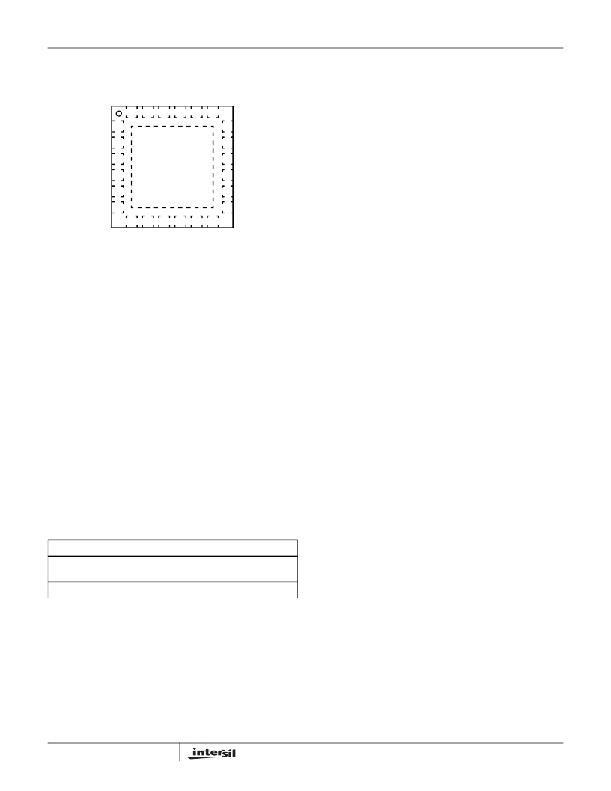 �
�
�ISL8510�
�Pin� Descriptions�
�In� addition,� the� PWM� regulator� power-good� and� undervoltage�
�protection� circuitry� use� FB_PWM� to� monitor� the� regulator�
�output� voltage.�
�24�
�23�
�22�
�21�
�20�
�19�
�PHASE�
�FB_LDO� 1�
�VOUT� 2�
�18� VIN�
�17� VIN�
�Switch� node� connections� to� internal� power� MOSFET� source,�
�external� output� inductor,� and� external� diode� cathode.�
�VIN_LDO� 3�
�GND� 4�
�GND� 5�
�NC� 6�
�25�
�GND�
�16� PHASE�
�15� PHASE�
�14� BOOT�
�13� PVCC�
�BOOT�
�Floating� bootstrap� supply� pin� for� the� power� MOSFET� gate�
�driver.� The� bootstrap� capacitor� provides� the� necessary�
�charge� to� turn� and� hold� on� the� internal� N-Channel� MOSFET.�
�Connect� an� external� capacitor� from� this� pin� to� PHASE.�
�7�
�8�
�9�
�10�
�11�
�12�
�EN�
�PWM� controller� enable� input.� The� PWM� converter� and�
�LDO's� outputs� are� held� off� when� the� pin� is� pulled� to� ground.�
�When� the� voltage� on� this� pin� is� logic� high,� the� chip� is�
�VIN�
�The� input� supply� for� the� PWM� regulator� power� stage� and� the�
�source� for� the� internal� linear� regulator� that� provides� bias� for�
�the� IC.� Place� a� ceramic� capacitor� from� VIN� to� GND� close� to�
�the� IC� for� decoupling� (typical� 1μF).�
�PVCC�
�Connect� this� pin� to� VCC.�
�GND�
�Ground� connect� for� the� IC� and� thermal� relief� for� the� package.�
�The� exposed� pad� must� be� connected� to� GND� and� soldered�
�to� the� PCB.� All� voltage� levels� are� measured� with� respect� to�
�this� pin.�
�VCC�
�Internal� 5V� linear� regulator� output� provides� bias� to� all� the�
�internal� control� logic.� The� ISL8510� may� be� powered� directly�
�from� a� 5V� (±10%)� supply� at� this� pin.� When� used� as� a� 5V� supply�
�input,� this� pin� must� be� externally� connected� to� VIN.� The� VCC�
�pin� must� always� be� decoupled� to� GND� with� a� ceramic� bypass�
�capacitor� (minimum� 1μF)� located� close� to� the� pin.�
�TABLE� 1.� INPUT� SUPPLY� CONFIGURATION�
�enabled.�
�SS�
�Program� pin� for� soft-start� duration.� A� regulated� 30μA� pull-up�
�current� source� charges� a� capacitor� connected� from� the� pin� to�
�GND.� The� output� voltage� of� the� converter� follows� the� ramping�
�voltage� on� the� SS� pin.�
�VIN_LDO�
�Input� voltage� pin� for� LDO.�
�VOUT�
�LDO� output� pin.� Bypass� with� a� minimum� of� 2.2� μ� F,� low� ESR�
�capacitor� to� GND� for� stable� operation.�
�FB_LDO�
�Used� to� set� the� output� of� LDO� with� the� proper� selection� of�
�resistor� divider.� The� resistors� should� be� selected� to� provide� a�
�minimum� current� of� 200nA� load� for� the� LDO.�
�CC�
�Compensation� capacitor� connection� for� LDO.� Connect� a�
�0.033μF� capacitor� from� pin� to� ground.�
�EN_LDO�
�INPUT�
�PIN� CONFIGURATION�
�The� pin� is� threshold-sensitive� enable� input� for� the� LDO.� Held�
�5.5V� to� 25V� Connect� the� input� supply� to� the� VIN� pin� only.� The� VCC� pin�
�will� provide� a� 5V� output� from� the� internal� linear� regulator.�
�low,� this� pin� disables� LDO.�
�PG_PWM�
�5V� ±10%�
�Connect� the� input� supply� to� the� VIN� and� VCC� pins.�
�PWM� converter� power-good� output.� Open� drain� logic� output�
�FB� _PWM� AND� COMP�
�The� standard� buck� regulator� employs� a� single� voltage� control�
�loop.� FB_PWM� is� the� negative� input� to� the� voltage� loop� error�
�amplifier.� COMP� is� the� output� of� the� error� amplifier.� The� output�
�voltage� is� set� by� an� external� resistor� divider� connected� to�
�FB_PWM.� With� a� properly� selected� divider,� the� output� voltage�
�can� be� set� to� any� voltage� between� the� power� rail� (reduced� by�
�converter� losses)� and� the� 0.6V� reference.� Connecting� an� AC�
�network� across� COMP� and� FB_PWM� provides� loop�
�compensation� to� the� amplifier.�
�8�
�that� is� pulled� to� ground� when� the� output� voltage� is� outside�
�regulation� limits.� Connect� a� 100k� Ω� resistor� from� this� pin� to�
�VCC.� Pin� is� low� when� the� buck� regulator� output� voltage� is�
�not� within� 10%� of� the� respective� nominal� voltage,� or� during�
�the� soft-start� interval.� Pin� is� high� impedance� when� the� output�
�is� within� regulation.�
�PG_LDO�
�Combined� LDO� power--good� output.� Connect� a� 100k� Ω� resistor�
�from� this� pin� to� VCC.�
�FN6516.2�
�December� 15,� 2008�
�相关PDF资料 |
PDF描述 |
|---|---|
| REC3-0505SRW/H6/A | CONV DC/DC 3W 4.5-9VIN 05VOUT |
| V110C3V3H50B3 | CONVERTER MOD DC/DC 3.3V 50W |
| F951C226KQAAQ2 | CAP TANT 22UF 16V 10% 1206 |
| ISL6549CRZ-T | IC REG DL BCK/LINEAR SYNC 16-QFN |
| UH4PBC-M3/86A | DIODE 4A 100V 25NS DUAL TO277A |
相关代理商/技术参数 |
参数描述 |
|---|---|
| ISL85402EVAL1Z | 制造商:Intersil Corporation 功能描述:ISL85402 EVAL BOARD1 - 20LD QFN - INPUT VOLTAGE 36V, 2.5A - Bulk |
| ISL85402IRZ | 功能描述:IC REG BUCK BOOST SYNC ADJ 20QFN RoHS:是 类别:集成电路 (IC) >> PMIC - 稳压器 - DC DC 开关稳压器 系列:- 产品培训模块:Lead (SnPb) Finish for COTS Obsolescence Mitigation Program 标准包装:2,500 系列:- 类型:降压(降压) 输出类型:两者兼有 输出数:1 输出电压:5V,1 V ~ 10 V 输入电压:3.5 V ~ 28 V PWM 型:电流模式 频率 - 开关:220kHz ~ 1MHz 电流 - 输出:600mA 同步整流器:无 工作温度:-40°C ~ 125°C 安装类型:表面贴装 封装/外壳:16-SSOP(0.154",3.90mm 宽) 包装:带卷 (TR) 供应商设备封装:16-QSOP |
| ISL85402IRZ-T | 功能描述:IC REG BUCK BOOST SYNC ADJ 20QFN RoHS:是 类别:集成电路 (IC) >> PMIC - 稳压器 - DC DC 开关稳压器 系列:- 产品培训模块:Lead (SnPb) Finish for COTS Obsolescence Mitigation Program 标准包装:2,500 系列:- 类型:降压(降压) 输出类型:两者兼有 输出数:1 输出电压:5V,1 V ~ 10 V 输入电压:3.5 V ~ 28 V PWM 型:电流模式 频率 - 开关:220kHz ~ 1MHz 电流 - 输出:600mA 同步整流器:无 工作温度:-40°C ~ 125°C 安装类型:表面贴装 封装/外壳:16-SSOP(0.154",3.90mm 宽) 包装:带卷 (TR) 供应商设备封装:16-QSOP |
| ISL85402IRZ-T7A | 功能描述:直流/直流开关调节器 SWITCHING REG 4X4 QFN RoHS:否 制造商:International Rectifier 最大输入电压:21 V 开关频率:1.5 MHz 输出电压:0.5 V to 0.86 V 输出电流:4 A 输出端数量: 最大工作温度: 安装风格:SMD/SMT 封装 / 箱体:PQFN 4 x 5 |
| ISL85402IRZ-TK | 功能描述:IC REG BUCK BOOST SYNC ADJ 20QFN RoHS:是 类别:集成电路 (IC) >> PMIC - 稳压器 - DC DC 开关稳压器 系列:- 产品培训模块:Lead (SnPb) Finish for COTS Obsolescence Mitigation Program 标准包装:2,500 系列:- 类型:降压(降压) 输出类型:两者兼有 输出数:1 输出电压:5V,1 V ~ 10 V 输入电压:3.5 V ~ 28 V PWM 型:电流模式 频率 - 开关:220kHz ~ 1MHz 电流 - 输出:600mA 同步整流器:无 工作温度:-40°C ~ 125°C 安装类型:表面贴装 封装/外壳:16-SSOP(0.154",3.90mm 宽) 包装:带卷 (TR) 供应商设备封装:16-QSOP |
发布紧急采购,3分钟左右您将得到回复。