- 您现在的位置:买卖IC网 > PDF目录16320 > ISL98003CNZ-EVALZ (Intersil)EVAL BOARD FOR ISL98003CNZ PDF资料下载
参数资料
| 型号: | ISL98003CNZ-EVALZ |
| 厂商: | Intersil |
| 文件页数: | 5/31页 |
| 文件大小: | 0K |
| 描述: | EVAL BOARD FOR ISL98003CNZ |
| 标准包装: | 1 |
| 系列: | * |
第1页第2页第3页第4页当前第5页第6页第7页第8页第9页第10页第11页第12页第13页第14页第15页第16页第17页第18页第19页第20页第21页第22页第23页第24页第25页第26页第27页第28页第29页第30页第31页
13
FN6760.0
September 12, 2008
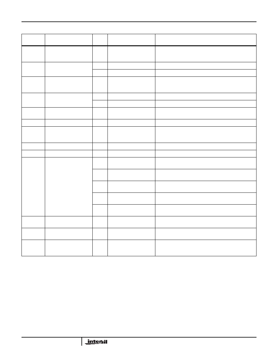
0x1A
Green Offset MSB, (0x80)
7:0
Green Offset MSB
ABLC off: upper 8 bits to Green offset DAC
ABLC enabled: Green digital offset
(See Red Offset)
0x1B
Green Offset LSB, (0x00)
5:0
N/A
7:6
Green Offset LSB
See Red Offset
0x1C
Blue Offset MSB, (0x80)
7:0
Blue Offset MSB
ABLC off: upper 8 bits to Blue offset DAC
ABLC enabled: Blue digital offset
(See Red Offset)
0x1D
Blue Offset LSB, (0x00)
5:0
N/A
7:6
Blue Offset LSB
See Red Offset
0x1E
PLL HTOTAL MSB, (0x06)
5:0
PLL HTOTAL MSB
14-bit HTOTAL
PLL updated on LSB write only.
0x1F
PLL HTOTAL LSB, (0x98)
7:0
PLL HTOTAL LSB
PLL updated on LSB write only. SXGA default
0x20
PLL Phase, (0x00)
5:0
PLL Sampling Phase
Used to control the phase of the ADC’s sample point relative
to the period of a pixel. Adjust to obtain optimum image quality.
One step = 5.625° (1.56% of pixel period).
0x21
PLL Pre-coast, (0x04)
7:0
Pre-coast
Number of lines the PLL will coast prior to the start of VSYNC.
0x22
PLL Post-coast, (0x04)
7:0
Post-coast
Number of lines the PLL will coast after the end of VSYNC.
0x23
PLL Misc, (0x00)
0
PLL Lock Edge HSYNC
0: PLL locks to trailing edge of selected HSYNC (default)
1: PLL locks to leading edge of selected HSYNC
1
CLKINV ENABLE
0: CLKINV input ignored
1: CLKINV input enabled
2
Ext Coast SEL
0: Internal COAST generation
1: External COAST source
3
Ext Coast POL
0: Active high external COAST
1: Active low external COAST
4
EXT CLOCK
0: Internal pixel clock from DPLL
1: External pixel clock from EXTCLKin pin
0x24
DC-Restore and ABLC
starting pixel MSB, (0x00)
5:0
DC-Restore and ABLC
starting pixel (MSB)
Pixel after Raw HSYNC trailing edge to begin DC-restore and
ABLC. 14 bits.
0x25
DC-Restore and ABLC
starting pixel LSB, (0x02)
7:0
DC-Restore and ABLC
starting pixel (LSB)
0x26
DC-Restore Clamp Width,
(0x10)
7:0
DC-Restore clamp width
Only applies to DC-restore clamp used for AC-coupled
configurations. A value of 0x00 means the clamp DAC is never
connected to the input.
Register Listing (Continued)
ADDRESS
REGISTER
(DEFAULT VALUE)
BITS
FUNCTION NAME
DESCRIPTION
ISL98003
相关PDF资料 |
PDF描述 |
|---|---|
| VE-J1T-EZ-F3 | CONVERTER MINIMOD DC/DC 6.5V 25W |
| 3-1906013-3 | CA 2.0MM OFNR 50/125,LC SEC BLU |
| A1RXB-2636G | IDC CABLE - APR26B/AE26G/X |
| EET-ED2W151BA | CAP ALUM 150UF 450V 20% SNAP |
| A3BRB-2018G | IDC CABLE - ASR20B/AE20G/APR20B |
相关代理商/技术参数 |
参数描述 |
|---|---|
| ISL98003INZ-110 | 功能描述:IC AFE 3CH 8BIT 110MHZ 80EPTQFP RoHS:是 类别:集成电路 (IC) >> 数据采集 - 模拟前端 (AFE) 系列:- 产品培训模块:Lead (SnPb) Finish for COTS Obsolescence Mitigation Program 标准包装:2,500 系列:- 位数:- 通道数:2 功率(瓦特):- 电压 - 电源,模拟:3 V ~ 3.6 V 电压 - 电源,数字:3 V ~ 3.6 V 封装/外壳:32-VFQFN 裸露焊盘 供应商设备封装:32-QFN(5x5) 包装:带卷 (TR) |
| ISL98003INZ-EVALZ | 功能描述:EVALUATION BOARD FOR ISL98003INZ RoHS:是 类别:编程器,开发系统 >> 评估演示板和套件 系列:- 标准包装:1 系列:PCI Express® (PCIe) 主要目的:接口,收发器,PCI Express 嵌入式:- 已用 IC / 零件:DS80PCI800 主要属性:- 次要属性:- 已供物品:板 |
| ISL98012IUZ | 功能描述:直流/直流开关转换器 1.8V INPUT PWM STP UPG 10LD RoHS:否 制造商:STMicroelectronics 最大输入电压:4.5 V 开关频率:1.5 MHz 输出电压:4.6 V 输出电流:250 mA 输出端数量:2 最大工作温度:+ 85 C 安装风格:SMD/SMT |
| ISL98012IUZ-T | 功能描述:IC REG BOOST ADJ 0.6A 10MSOP RoHS:是 类别:集成电路 (IC) >> PMIC - 稳压器 - DC DC 开关稳压器 系列:- 产品培训模块:Lead (SnPb) Finish for COTS Obsolescence Mitigation Program 标准包装:2,500 系列:- 类型:降压(降压) 输出类型:两者兼有 输出数:1 输出电压:5V,1 V ~ 10 V 输入电压:3.5 V ~ 28 V PWM 型:电流模式 频率 - 开关:220kHz ~ 1MHz 电流 - 输出:600mA 同步整流器:无 工作温度:-40°C ~ 125°C 安装类型:表面贴装 封装/外壳:16-SSOP(0.154",3.90mm 宽) 包装:带卷 (TR) 供应商设备封装:16-QSOP |
| ISL98012IUZ-TK | 功能描述:IC REG BOOST ADJ 0.6A 10MSOP RoHS:是 类别:集成电路 (IC) >> PMIC - 稳压器 - DC DC 开关稳压器 系列:- 标准包装:1 系列:EZBuck™ 类型:降压(降压) 输出类型:可调式 输出数:1 输出电压:0.8 V ~ 22.1 V 输入电压:3 V ~ 26 V PWM 型:电流模式 频率 - 开关:1.5MHz 电流 - 输出:1.8A 同步整流器:无 工作温度:-40°C ~ 85°C 安装类型:表面贴装 封装/外壳:8-WFDFN 裸露焊盘 包装:剪切带 (CT) 供应商设备封装:8-DFN(2x2) 其它名称:785-1276-1 |
发布紧急采购,3分钟左右您将得到回复。