参数资料
| 型号: | ISLA222P13IRZ |
| 厂商: | Intersil |
| 文件页数: | 16/33页 |
| 文件大小: | 0K |
| 描述: | IC ADC 12BIT SRL/SPI 72QFN |
| 标准包装: | 1 |
| 系列: | FemtoCharge™ |
| 位数: | 12 |
| 采样率(每秒): | 130M |
| 数据接口: | 串行,SPI? |
| 转换器数目: | 2 |
| 功率耗散(最大): | 697mW |
| 电压电源: | 模拟和数字 |
| 工作温度: | -40°C ~ 85°C |
| 安装类型: | 表面贴装 |
| 封装/外壳: | 72-VFQFN 裸露焊盘 |
| 供应商设备封装: | 72-QFN(10x10) |
| 包装: | 托盘 |
| 输入数目和类型: | * |
第1页第2页第3页第4页第5页第6页第7页第8页第9页第10页第11页第12页第13页第14页第15页当前第16页第17页第18页第19页第20页第21页第22页第23页第24页第25页第26页第27页第28页第29页第30页第31页第32页第33页
ISLA222P
23
FN7853.1
June 17, 2011
Serial Peripheral Interface
A serial peripheral interface (SPI) bus is used to facilitate
configuration of the device and to optimize performance. The SPI
bus consists of chip select (CSB), serial clock (SCLK) serial data
output (SDO), and serial data input/output (SDIO). The maximum
SCLK rate is equal to the A/D sample rate (fSAMPLE) divided by 32
for write operations and fSAMPLE divided by 132 for reads. At
fSAMPLE = 250MHz, maximum SCLK is 15.63MHz for writing and
3.79MHz for read operations. There is no minimum SCLK rate.
The following sections describe various registers that are used to
configure the SPI or adjust performance or functional parameters.
Many registers in the available address space (0x00 to 0xFF) are
not defined in this document. Additionally, within a defined
register there may be certain bits or bit combinations that are
reserved. Undefined registers and undefined values within defined
registers are reserved and should not be selected. Setting any
reserved register or value may produce indeterminate results.
SPI Physical Interface
The serial clock pin (SCLK) provides synchronization for the data
transfer. By default, all data is presented on the serial data
input/output (SDIO) pin in three-wire mode. The state of the SDIO
pin is set automatically in the communication protocol
(described in the following). A dedicated serial data output pin
(SDO) can be activated by setting 0x00[7] high to allow operation
in four-wire mode.
The SPI port operates in a half duplex master/slave
configuration, with the ISLA222P functioning as a slave. Multiple
slave devices can interface to a single master in three-wire mode
only, since the SDO output of an unaddressed device is asserted
in four wire mode.
The chip-select bar (CSB) pin determines when a slave device is
being addressed. Multiple slave devices can be written to
concurrently, but only one slave device can be read from at a
given time (again, only in three-wire mode). If multiple slave
devices are selected for reading at the same time, the results will
be indeterminate.
The communication protocol begins with an instruction/address
phase. The first rising SCLK edge following a high-to-low
transition on CSB determines the beginning of the two-byte
instruction/address command; SCLK must be static low before
the CSB transition. Data can be presented in MSB-first order or
LSB-first order. The default is MSB-first, but this can be changed
bit ordering for the MSB-first and LSB-first modes, respectively. In
MSB-first mode, the address is incremented for multi-byte
transfers, while in LSB-first mode it’s decremented.
In the default mode, the MSB is R/W, which determines if the
data is to be read (active high) or written. The next two bits, W1
and W0, determine the number of data bytes to be read or
written (see Table 4). The lower 13 bits contain the first address
for the data transfer. This relationship is illustrated in Figure 38,
and timing values are given in “Switching Specifications” on
After the instruction/address bytes have been read, the
appropriate number of data bytes are written to or read from the
A/D (based on the R/W bit status). The data transfer will
continue as long as CSB remains low and SCLK is active. Stalling
of the CSB pin is allowed at any byte boundary
(instruction/address or data) if the number of bytes being
transferred is three or less. For transfers of four bytes or more,
CSB is allowed to stall in the middle of the instruction/address
bytes or before the first data byte. If CSB transitions to a high
state after that point the state machine will reset and terminate
the data transfer.
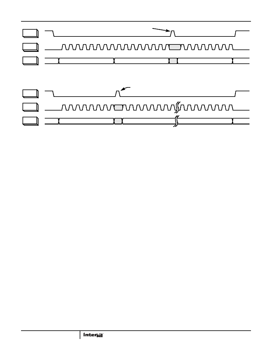
FIGURE 40. 2-BYTE TRANSFER
CSB
SCLK
SDIO
INSTRUCTION/ADDRESS
DATA WORD 1
DATA WORD 2
CSB STALLING
FIGURE 41. N-BYTE TRANSFER
CSB
SCLK
SDIO
INSTRUCTION/ADDRESS
DATA WORD 1
DATA WORD N
LAST LEGAL
CSB STALLING
相关PDF资料 |
PDF描述 |
|---|---|
| ISLA224S25IR1Z | IC ADC |
| KAD2708C-27Q68 | IC ADC 8BIT 275MSPS PAR 68-QFN |
| KAD2708L-27Q68 | IC ADC 8BIT 275MSPS PAR 68-QFN |
| KAD2710C-27Q68 | IC ADC 10BIT 275MSPS PAR 68-QFN |
| KAD2710L-21Q68 | IC ADC 10BIT 210MSPS SGL 68-QFN |
相关代理商/技术参数 |
参数描述 |
|---|---|
| ISLA222P20 | 制造商:INTERSIL 制造商全称:Intersil Corporation 功能描述:Dual 14-Bit, 250MSPS/200MSPS/130MSPS ADC |
| ISLA222P20IRZ | 功能描述:IC ADC 12BIT SRL/SPI 72QFN RoHS:是 类别:集成电路 (IC) >> 数据采集 - 模数转换器 系列:FemtoCharge™ 产品培训模块:Lead (SnPb) Finish for COTS Obsolescence Mitigation Program 标准包装:1 系列:- 位数:10 采样率(每秒):357k 数据接口:DSP,MICROWIRE?,QSPI?,串行,SPI? 转换器数目:1 功率耗散(最大):830µW 电压电源:单电源 工作温度:-40°C ~ 85°C 安装类型:表面贴装 封装/外壳:10-WFDFN 裸露焊盘 供应商设备封装:10-TDFN-EP(3x3) 包装:剪切带 (CT) 输入数目和类型:2 个单端,单极;2 个单端,双极;1 个差分,单极;1 个差分,双极 产品目录页面:1396 (CN2011-ZH PDF) 其它名称:MAX1395ETB+TCT |
| ISLA222P25 | 制造商:INTERSIL 制造商全称:Intersil Corporation 功能描述:Dual 14-Bit, 250MSPS/200MSPS/130MSPS ADC |
| ISLA222P25IRZ | 制造商:Intersil Corporation 功能描述:12-BIT 250MSPS DUAL ADC, 72-PIN QFN - Trays 制造商:Intersil Corporation 功能描述:IC ADC 12BIT SRL/SPI 72QFN 制造商:Intersil 功能描述:12-BIT 250MSPS DL AD C 72-PIN |
| ISLA222S | 制造商:INTERSIL 制造商全称:Intersil Corporation 功能描述:Dual 12-Bit, 250/200/125 MSPS JESD204B High Speed Serial Output ADC |
发布紧急采购,3分钟左右您将得到回复。