参数资料
| 型号: | KAD5510P-25Q48 |
| 厂商: | Intersil |
| 文件页数: | 17/31页 |
| 文件大小: | 0K |
| 描述: | IC ADC 10BIT CMOS 250MSPS 48QFN |
| 标准包装: | 40 |
| 系列: | FemtoCharge™ |
| 位数: | 10 |
| 采样率(每秒): | 250M |
| 数据接口: | 串行,SPI? |
| 转换器数目: | 1 |
| 功率耗散(最大): | 254mW |
| 电压电源: | 单电源 |
| 工作温度: | -40°C ~ 85°C |
| 安装类型: | 表面贴装 |
| 封装/外壳: | 48-VFQFN 裸露焊盘 |
| 供应商设备封装: | 48-QFN(7x7) |
| 包装: | 托盘 |
| 输入数目和类型: | * |
第1页第2页第3页第4页第5页第6页第7页第8页第9页第10页第11页第12页第13页第14页第15页第16页当前第17页第18页第19页第20页第21页第22页第23页第24页第25页第26页第27页第28页第29页第30页第31页
KAD5510P
24
FN7693.2
May 2, 2011
ADDRESS 0X74: OUTPUT_MODE_B
ADDRESS 0X75: CONFIG_STATUS
Bit 6 DLL Range
This bit sets the DLL operating range to fast (default) or slow.
Internal clock signals are generated by a delay-locked loop (DLL),
which has a finite operating range. Table 11 shows the allowable
sample rate ranges for the slow and fast settings.
The output_mode_B and config_status registers are used in
conjunction to enable DDR mode and select the frequency range
of the DLL clock generator. The method of setting these options
is different from the other registers.
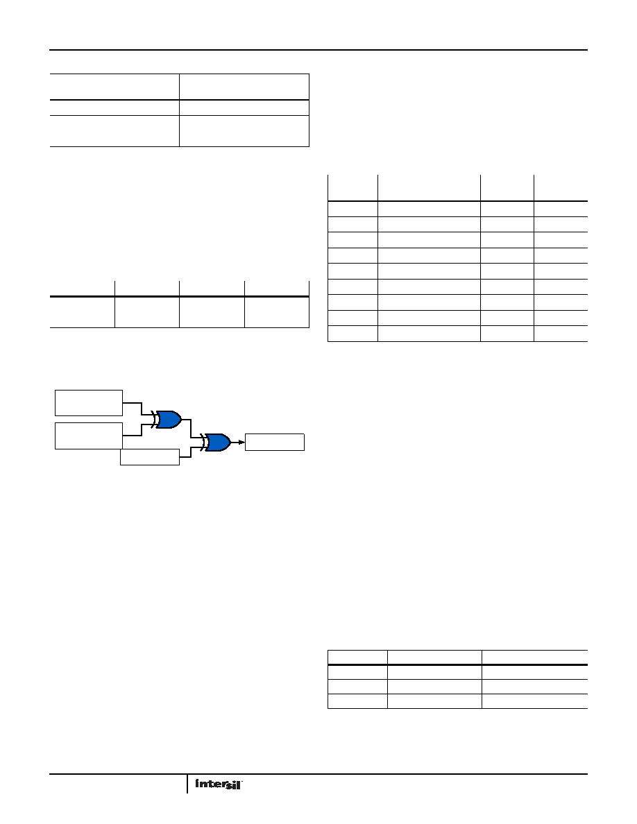
The procedure for setting output_mode_B is shown in Figure 41.
Read the contents of output_mode_B and config_status and XOR
them. Then XOR this result with the desired value for
output_mode_B and write that XOR result to the register.
Bit 4 DDR Enable
This bit sets the output mode to DDR or SDR.
This bit is set high by default enabling DDR outputs. Do not set
this bit low or invalid output data will result.
Device Test
The KAD5510 can produce preset or user defined patterns on the
digital outputs to facilitate in-site testing. A static word can be
placed on the output bus, or two different words can alternate. In
the alternate mode, the values defined as Word 1 and Word 2 (as
shown in Table 12) are set on the output bus on alternating clock
phases. The test mode is enabled asynchronously to the sample
clock, therefore several sample clock cycles may elapse before
the data is present on the output bus.
ADDRESS 0XC0: TEST_IO
Bits 7:6 User Test Mode
These bits set the test mode to static (0x00) or alternate
(0x01) mode. Other values are reserved.
The four LSBs in this register (Output Test Mode) determine the
test pattern in combination with registers 0xC2 through 0xC5.
Refer to Table 12.
ADDRESS 0XC2: USER_PATT1_LSB AND
ADDRESS 0XC3: USER_PATT1_MSB
These registers define the lower and upper eight bits,
respectively, of the first user-defined test word.
ADDRESS 0XC4: USER_PATT2_LSB AND
ADDRESS 0XC5: USER_PATT2_MSB
These registers define the lower and upper eight bits,
respectively, of the second user-defined test word.
48 Pin Package Notes
The KAD5510 is only available in a 48-pin package. While fully
compatible with other family members in the 48-pin package
there are some key differences from the 72-pin package. The 48
pin package option supports LVDS DDR only. A reduced set of pin
selectable functions are available in the 48 pin package due to
the reduced pinout; (OUTMODE, OUTFMT, and CLKDIV pins are
not available). Table 13 shows the default state for these
functions for the 48-pin package. Note that these functions are
available through the SPI, allowing a user to set these modes as
they desire, offering the same flexibility as the 72-pin family
members.
001
Two’s Complement
010
Gray Code
100
Offset Binary
TABLE 11. DLL RANGES
DLL RANGE
MIN
MAX
UNIT
Slow
40
100
MSPS
Fast
80
fS MAX
MSPS
TABLE 10. OUTPUT FORMAT CONTROL
(Continued)
VALUE
0x93[2:0]
OUTPUT FORMAT
FIGURE 41. SETTING OUTPUT_MODE_B REGISTER
READ
CONFIG_STATUS
0x75
READ
OUTPUT_MODE_B
0x74
DESIRED
VALUE
WRITE TO
0x74
TABLE 12. OUTPUT TEST MODES
VALUE
0xC0[3:0]
OUTPUT TEST MODE
WORD 1
WORD 2
0000
Off
0001
Midscale
0x8000
N/A
0010
Positive Full-Scale
0xFFFF
N/A
0011
Negative Full-Scale
0x0000
N/A
0100
Checkerboard
0xAAAA
0x5555
0101
Reserved
N/A
0110
Reserved
N/A
0111
One/Zero
0xFFFF
0x0000
1000
User Pattern
user_patt1
user_patt2
TABLE 13. 48 PIN SPI - ADDRESSABLE FUNCTIONS
FUNCTION
DESCRIPTION
DEFAULT STATE
CLKDIV
Clock Divider
Divide by 1
OUTMODE
Output Driver Mode
LVDS, 3mA (DDR)
OUTFMT
Data Coding
Two’s Complement
相关PDF资料 |
PDF描述 |
|---|---|
| KAD5510P-50Q72 | IC ADC 10BIT 500MSPS SGL 72-QFN |
| KAD5512HP-17Q72 | IC ADC 12BIT 170MSPS SGL 72-QFN |
| KAD5512P-17Q72 | IC ADC 12BIT 170MSPS SGL 72-QFN |
| KAD5514P-12Q72 | IC ADC 14BIT 125MSPS SGL 72-QFN |
| KAD5610P-25Q72 | IC ADC 10BIT 250MSPS DUAL 72-QFN |
相关代理商/技术参数 |
参数描述 |
|---|---|
| KAD5510P-50 | 制造商:未知厂家 制造商全称:未知厂家 功能描述:10-Bit, 500MSPS A/D Converter |
| KAD5510P-50_09 | 制造商:INTERSIL 制造商全称:Intersil Corporation 功能描述:10-Bit, 500MSPS A/D Converter |
| KAD5510P-50_0910 | 制造商:INTERSIL 制造商全称:Intersil Corporation 功能描述:10-Bit, 500MSPS A/D Converter |
| KAD5510P-50Q72 | 功能描述:IC ADC 10BIT 500MSPS SGL 72-QFN RoHS:是 类别:集成电路 (IC) >> 数据采集 - 模数转换器 系列:FemtoCharge™ 产品培训模块:Lead (SnPb) Finish for COTS Obsolescence Mitigation Program 标准包装:250 系列:- 位数:12 采样率(每秒):1.8M 数据接口:并联 转换器数目:1 功率耗散(最大):1.82W 电压电源:模拟和数字 工作温度:-40°C ~ 85°C 安装类型:表面贴装 封装/外壳:48-LQFP 供应商设备封装:48-LQFP(7x7) 包装:管件 输入数目和类型:2 个单端,单极 |
| KAD5512HP | 制造商:未知厂家 制造商全称:未知厂家 功能描述:High Performance 12-Bit, 250/210/170/125MSPS ADC |
发布紧急采购,3分钟左右您将得到回复。