参数资料
| 型号: | KAD5512P-12Q72 |
| 厂商: | Intersil |
| 文件页数: | 13/36页 |
| 文件大小: | 0K |
| 描述: | IC ADC 12BIT 125MSPS SGL 72-QFN |
| 产品培训模块: | High-Speed Analog-to-Digital Converters |
| 标准包装: | 1 |
| 系列: | FemtoCharge™ |
| 位数: | 12 |
| 采样率(每秒): | 125M |
| 数据接口: | 串行,SPI? |
| 转换器数目: | 1 |
| 功率耗散(最大): | 235mW |
| 电压电源: | 单电源 |
| 工作温度: | -40°C ~ 85°C |
| 安装类型: | 表面贴装 |
| 封装/外壳: | 72-VFQFN 裸露焊盘 |
| 供应商设备封装: | 72-QFN(10x10) |
| 包装: | 托盘 |
| 输入数目和类型: | 1 个差分,单极 |
第1页第2页第3页第4页第5页第6页第7页第8页第9页第10页第11页第12页当前第13页第14页第15页第16页第17页第18页第19页第20页第21页第22页第23页第24页第25页第26页第27页第28页第29页第30页第31页第32页第33页第34页第35页第36页
KAD5512P
20
FN6807.4
October 1, 2010
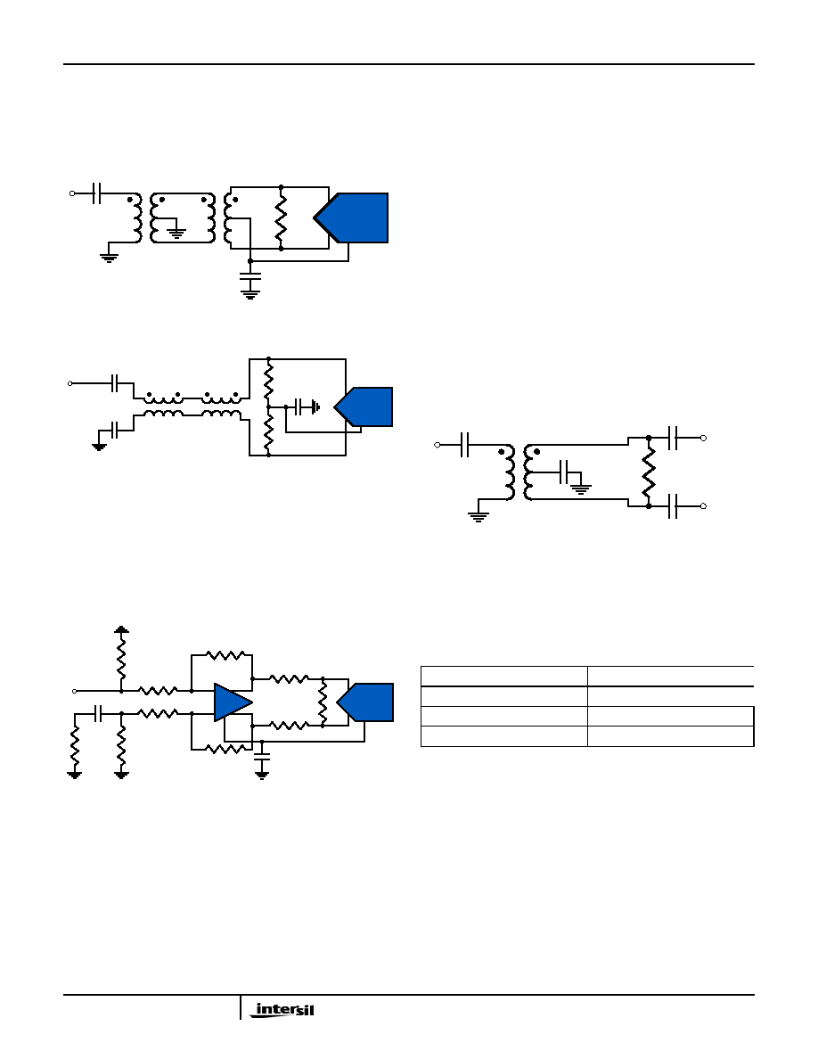
This dual transformer scheme is used to improve common-
mode rejection, which keeps the common-mode level of
the input matched to VCM. The value of the shunt resistor
should be determined based on the desired load
impedance. The differential input resistance of the
KAD5512P is 1000Ω.
The SHA design uses a switched capacitor input stage
(see Figure 43), which creates current spikes when the
sampling capacitance is reconnected to the input voltage.
This causes a disturbance at the input which must settle
before the next sampling point. Lower source impedance
will result in faster settling and improved performance.
Therefore a 1:1 transformer and low shunt resistance are
recommended for optimal performance.
A differential amplifier, as shown in Figure 30, can be
used in applications that require DC-coupling. In this
configuration, the amplifier will typically dominate the
achievable SNR and distortion performance.
The current spikes from the SHA will try to force the
analog input pins toward ground. In cases where the
input pins are biased with more than 50Ω in series from
VCM care must be taken to make sure the input common
mode range is not violated. The provided ICM value
(250A/MHz * 250MHz = 625A at 250MSPS) may be
used to calculate the expected voltage drop across any
series resistance.
VCM Output
The VCM output is buffered with a series output
impedance of 20Ω. It can easily drive a typical ADC
driver’s 10kΩ common mode control pin. If an external
buffer is not used the voltage drop across the internal
20Ω impedance must be considered when calculating the
expected DC bias voltage at the analog input pins.
Clock Input
The clock input circuit is a differential pair (see
Figure 44). Driving these inputs with a high level (up to
1.8VPP on each input) sine or square wave will provide
the lowest jitter performance. A transformer with 4:1
impedance ratio will provide increased drive levels.
The recommended drive circuit is shown in Figure 31. A
duty range of 40% to 60% is acceptable. The clock can
be driven single-ended, but this will reduce the edge rate
and may impact SNR performance. The clock inputs are
internally self-biased to AVDD/2 to facilitate AC coupling.
A selectable 2x frequency divider is provided in series
with the clock input. The divider can be used in the 2x
mode with a sample clock equal to twice the desired
sample rate. This allows the use of the Phase Slip
feature, which enables synchronization of multiple ADCs.
The clock divider can also be controlled through the SPI
port, which overrides the CLKDIV pin setting. Details on this
are contained in “Serial Peripheral Interface” on page 24.
A delay-locked loop (DLL) generates internal clock
signals for various stages within the charge pipeline. If
the frequency of the input clock changes, the DLL may
take up to 52s to regain lock at 250MSPS. The lock time
is inversely proportional to the sample rate.
Jitter
In a sampled data system, clock jitter directly impacts
the achievable SNR performance. The theoretical
relationship between clock jitter (tJ) and SNR is shown in
FIGURE 28. TRANSFORMER INPUT FOR GENERAL
PURPOSE APPLICATIONS
ADT1-1WT
0.1F
KAD5512P
VCM
ADT1-1WT
1000pF
FIGURE 29. TRANSMISSION-LINE TRANSFORMER
INPUT FOR HIGH IF APPLICATIONS
ADTL1-12
0.1F
KAD5512P
VCM
ADTL1-12
1000pF
KAD5512P
VCM
0.1F
0.22F
69.8
49.9
100
348
CM
217
25
69.8
FIGURE 30. DIFFERENTIAL AMPLIFIER INPUT
Ω
TABLE 1. CLKDIV PIN SETTINGS
CLKDIV PIN
DIVIDE RATIO
AVSS
2
Float
1
AVDD
4
FIGURE 31. RECOMMENDED CLOCK DRIVE
TC4-1W
200pF
200O
200pF
CLKP
CLKN
1000pF
Ω
相关PDF资料 |
PDF描述 |
|---|---|
| MS27499E10F35SB | CONN RCPT 13POS BOX MNT W/SCKT |
| V24B24M250BL2 | CONVERTER MOD DC/DC 24V 250W |
| IDT82V2041EPP | IC LIU T1/J1/E1 1CH 44-TQFP |
| IDT82V2042EPFG8 | IC LIU T1/J1/E1 2CH SHORT 80TQFP |
| V24B24M250BL | CONVERTER MOD DC/DC 24V 250W |
相关代理商/技术参数 |
参数描述 |
|---|---|
| KAD5512P-17Q48 | 功能描述:模数转换器 - ADC 12-BIT 170MSPS SINGL ADC PROG LVDS/LVCMOS RoHS:否 制造商:Texas Instruments 通道数量:2 结构:Sigma-Delta 转换速率:125 SPs to 8 KSPs 分辨率:24 bit 输入类型:Differential 信噪比:107 dB 接口类型:SPI 工作电源电压:1.7 V to 3.6 V, 2.7 V to 5.25 V 最大工作温度:+ 85 C 安装风格:SMD/SMT 封装 / 箱体:VQFN-32 |
| KAD5512P-17Q72 | 功能描述:模数转换器 - ADC 12-BIT 170MSPS SINGL ADC PROG LVDS/LVCMOS RoHS:否 制造商:Texas Instruments 通道数量:2 结构:Sigma-Delta 转换速率:125 SPs to 8 KSPs 分辨率:24 bit 输入类型:Differential 信噪比:107 dB 接口类型:SPI 工作电源电压:1.7 V to 3.6 V, 2.7 V to 5.25 V 最大工作温度:+ 85 C 安装风格:SMD/SMT 封装 / 箱体:VQFN-32 |
| KAD5512P-21Q48 | 功能描述:模数转换器 - ADC 12-BIT 210MSPS SINGL ADC PROG LVDS/LVCMOS RoHS:否 制造商:Texas Instruments 通道数量:2 结构:Sigma-Delta 转换速率:125 SPs to 8 KSPs 分辨率:24 bit 输入类型:Differential 信噪比:107 dB 接口类型:SPI 工作电源电压:1.7 V to 3.6 V, 2.7 V to 5.25 V 最大工作温度:+ 85 C 安装风格:SMD/SMT 封装 / 箱体:VQFN-32 |
| KAD5512P-21Q72 | 功能描述:模数转换器 - ADC 12-BIT 210MSPS SINGL ADC PROG LVDS/LVCMOS RoHS:否 制造商:Texas Instruments 通道数量:2 结构:Sigma-Delta 转换速率:125 SPs to 8 KSPs 分辨率:24 bit 输入类型:Differential 信噪比:107 dB 接口类型:SPI 工作电源电压:1.7 V to 3.6 V, 2.7 V to 5.25 V 最大工作温度:+ 85 C 安装风格:SMD/SMT 封装 / 箱体:VQFN-32 |
| KAD5512P-25Q48 | 功能描述:模数转换器 - ADC 12-BIT 250MSPS SINGL PROG LVDS/LVCMOS RoHS:否 制造商:Texas Instruments 通道数量:2 结构:Sigma-Delta 转换速率:125 SPs to 8 KSPs 分辨率:24 bit 输入类型:Differential 信噪比:107 dB 接口类型:SPI 工作电源电压:1.7 V to 3.6 V, 2.7 V to 5.25 V 最大工作温度:+ 85 C 安装风格:SMD/SMT 封装 / 箱体:VQFN-32 |
发布紧急采购,3分钟左右您将得到回复。