参数资料
| 型号: | KAD5512P-12Q72 |
| 厂商: | Intersil |
| 文件页数: | 18/36页 |
| 文件大小: | 0K |
| 描述: | IC ADC 12BIT 125MSPS SGL 72-QFN |
| 产品培训模块: | High-Speed Analog-to-Digital Converters |
| 标准包装: | 1 |
| 系列: | FemtoCharge™ |
| 位数: | 12 |
| 采样率(每秒): | 125M |
| 数据接口: | 串行,SPI? |
| 转换器数目: | 1 |
| 功率耗散(最大): | 235mW |
| 电压电源: | 单电源 |
| 工作温度: | -40°C ~ 85°C |
| 安装类型: | 表面贴装 |
| 封装/外壳: | 72-VFQFN 裸露焊盘 |
| 供应商设备封装: | 72-QFN(10x10) |
| 包装: | 托盘 |
| 输入数目和类型: | 1 个差分,单极 |
第1页第2页第3页第4页第5页第6页第7页第8页第9页第10页第11页第12页第13页第14页第15页第16页第17页当前第18页第19页第20页第21页第22页第23页第24页第25页第26页第27页第28页第29页第30页第31页第32页第33页第34页第35页第36页
KAD5512P
25
FN6807.4
October 1, 2010
Bit 7 SDO Active
Bit 6 LSB First
Setting this bit high configures the SPI to interpret
serial data as arriving in LSB to MSB order.
Bit 5 Soft Reset
Setting this bit high resets all SPI registers to default
values.
Bit 4 Reserved
This bit should always be set high.
Bits 3:0 These bits should always mirror bits 4:7 to
avoid ambiguity in bit ordering.
ADDRESS 0X02: BURST_END
If a series of sequential registers are to be set, burst
mode can improve throughput by eliminating redundant
addressing. In 3-wire SPI mode the burst is ended by
pulling the CSB pin high. If the device is operated in 2-
wire mode the CSB pin is not available. In that case,
setting the burst_end address determines the end of the
transfer. During a write operation, the user must be
cautious to transmit the correct number of bytes based
on the starting and ending addresses.
Bits 7:0 Burst End Address
This register value determines the ending address of
the burst data.
Device Information
ADDRESS 0X08: CHIP_ID
ADDRESS 0X09: CHIP_VERSION
The generic die identifier and a revision number,
respectively, can be read from these two registers.
Indexed Device Configuration/Control
ADDRESS 0X10: DEVICE_INDEX_A
A common SPI map, which can accommodate
single-channel or multi-channel devices, is used for all
Intersil ADC products. Certain configuration commands
(identified as Indexed in the SPI map) can be executed
on a per-converter basis. This register determines which
converter is being addressed for an Indexed command. It
is important to note that only a single converter can be
addressed at a time.
This register defaults to 00h, indicating that no ADC is
addressed. Therefore Bit 0 must be set high in order to
execute any Indexed commands. Error code ‘AD’ is
returned if any indexed register is read from without
properly setting device_index_A.
ADDRESS 0X20: OFFSET_COARSE AND
ADDRESS 0X21: OFFSET_FINE
The input offset of the ADC core can be adjusted in fine
and coarse steps. Both adjustments are made via an 8-
bit word as detailed in Table 7.
The default value of each register will be the result of the
self-calibration after initial power-up. If a register is to be
incremented or decremented, the user should first read
the register value then write the incremented or
decremented value back to the same register.
ADDRESS 0X22: GAIN_COARSE
ADDRESS 0X23: GAIN_MEDIUM
ADDRESS 0X24: GAIN_FINE
Gain of the ADC core can be adjusted in coarse,
medium and fine steps. Coarse gain is a 4-bit
adjustment while medium and fine are 8-bit. Multiple
Coarse Gain Bits can be set for a total adjustment
range of ±4.2% (‘0011’ =~ -4.2% and
‘1100’ =~ +4.2%). It is recommended to use one of
the coarse gain settings (-4.2%, -2.8%, -1.4%, 0,
1.4%, 2.8%, 4.2%) and fine-tune the gain using the
registers at 23h and 24h.
The default value of each register will be the result of the
self-calibration after initial power-up. If a register is to be
incremented or decremented, the user should first read
the register value then write the incremented or
decremented value back to the same register.
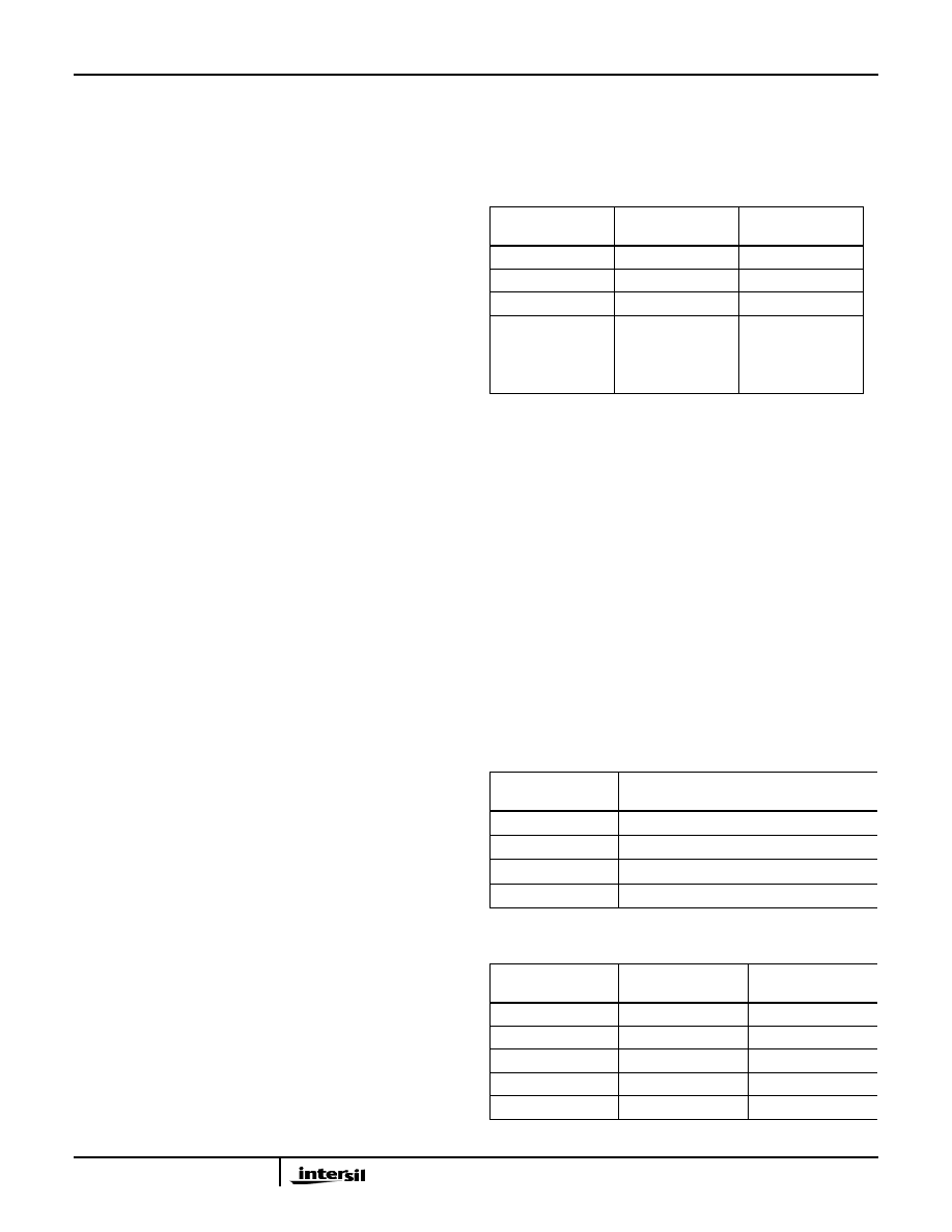
TABLE 7. OFFSET ADJUSTMENTS
PARAMETER
0x20[7:0]
COARSE OFFSET
0x21[7:0]
FINE OFFSET
Steps
255
–Full Scale (0x00) -133LSB (-47mV) -5LSB (-1.75mV)
Mid–Scale (0x80)
0.0LSB (0.0mV)
0.0LSB
+Full Scale (0xFF)
+133LSB
(+47mV)
+5LSB (+1.75mV)
Nominal Step Size 1.04LSB (0.37mV)
0.04LSB
(0.014mV)
TABLE 8. COARSE GAIN ADJUSTMENT
0x22[3:0]
NOMINAL COARSE GAIN ADJUST
(%)
Bit3
+2.8
Bit2
+1.4
Bit1
-2.8
Bit0
-1.4
TABLE 9. MEDIUM AND FINE GAIN ADJUSTMENTS
PARAMETER
0x23[7:0]
MEDIUM GAIN
0x24[7:0]
FINE GAIN
Steps
256
–Full Scale (0x00)
-2%
-0.20%
Mid–Scale (0x80)
0.00%
+Full Scale (0xFF)
+2%
+0.2%
Nominal Step Size
0.016%
0.0016%
相关PDF资料 |
PDF描述 |
|---|---|
| MS27499E10F35SB | CONN RCPT 13POS BOX MNT W/SCKT |
| V24B24M250BL2 | CONVERTER MOD DC/DC 24V 250W |
| IDT82V2041EPP | IC LIU T1/J1/E1 1CH 44-TQFP |
| IDT82V2042EPFG8 | IC LIU T1/J1/E1 2CH SHORT 80TQFP |
| V24B24M250BL | CONVERTER MOD DC/DC 24V 250W |
相关代理商/技术参数 |
参数描述 |
|---|---|
| KAD5512P-17Q48 | 功能描述:模数转换器 - ADC 12-BIT 170MSPS SINGL ADC PROG LVDS/LVCMOS RoHS:否 制造商:Texas Instruments 通道数量:2 结构:Sigma-Delta 转换速率:125 SPs to 8 KSPs 分辨率:24 bit 输入类型:Differential 信噪比:107 dB 接口类型:SPI 工作电源电压:1.7 V to 3.6 V, 2.7 V to 5.25 V 最大工作温度:+ 85 C 安装风格:SMD/SMT 封装 / 箱体:VQFN-32 |
| KAD5512P-17Q72 | 功能描述:模数转换器 - ADC 12-BIT 170MSPS SINGL ADC PROG LVDS/LVCMOS RoHS:否 制造商:Texas Instruments 通道数量:2 结构:Sigma-Delta 转换速率:125 SPs to 8 KSPs 分辨率:24 bit 输入类型:Differential 信噪比:107 dB 接口类型:SPI 工作电源电压:1.7 V to 3.6 V, 2.7 V to 5.25 V 最大工作温度:+ 85 C 安装风格:SMD/SMT 封装 / 箱体:VQFN-32 |
| KAD5512P-21Q48 | 功能描述:模数转换器 - ADC 12-BIT 210MSPS SINGL ADC PROG LVDS/LVCMOS RoHS:否 制造商:Texas Instruments 通道数量:2 结构:Sigma-Delta 转换速率:125 SPs to 8 KSPs 分辨率:24 bit 输入类型:Differential 信噪比:107 dB 接口类型:SPI 工作电源电压:1.7 V to 3.6 V, 2.7 V to 5.25 V 最大工作温度:+ 85 C 安装风格:SMD/SMT 封装 / 箱体:VQFN-32 |
| KAD5512P-21Q72 | 功能描述:模数转换器 - ADC 12-BIT 210MSPS SINGL ADC PROG LVDS/LVCMOS RoHS:否 制造商:Texas Instruments 通道数量:2 结构:Sigma-Delta 转换速率:125 SPs to 8 KSPs 分辨率:24 bit 输入类型:Differential 信噪比:107 dB 接口类型:SPI 工作电源电压:1.7 V to 3.6 V, 2.7 V to 5.25 V 最大工作温度:+ 85 C 安装风格:SMD/SMT 封装 / 箱体:VQFN-32 |
| KAD5512P-25Q48 | 功能描述:模数转换器 - ADC 12-BIT 250MSPS SINGL PROG LVDS/LVCMOS RoHS:否 制造商:Texas Instruments 通道数量:2 结构:Sigma-Delta 转换速率:125 SPs to 8 KSPs 分辨率:24 bit 输入类型:Differential 信噪比:107 dB 接口类型:SPI 工作电源电压:1.7 V to 3.6 V, 2.7 V to 5.25 V 最大工作温度:+ 85 C 安装风格:SMD/SMT 封装 / 箱体:VQFN-32 |
发布紧急采购,3分钟左右您将得到回复。