- 您现在的位置:买卖IC网 > PDF目录15745 > KIT908EINTFC (Freescale Semiconductor)KIT EVAL 908E625 QUAD W/MCU/LIN PDF资料下载
参数资料
| 型号: | KIT908EINTFC |
| 厂商: | Freescale Semiconductor |
| 文件页数: | 11/49页 |
| 文件大小: | 0K |
| 描述: | KIT EVAL 908E625 QUAD W/MCU/LIN |
| 标准包装: | 1 |
第1页第2页第3页第4页第5页第6页第7页第8页第9页第10页当前第11页第12页第13页第14页第15页第16页第17页第18页第19页第20页第21页第22页第23页第24页第25页第26页第27页第28页第29页第30页第31页第32页第33页第34页第35页第36页第37页第38页第39页第40页第41页第42页第43页第44页第45页第46页第47页第48页第49页
Analog Integrated Circuit Device Data
Freescale Semiconductor
19
908E625
FUNCTIONAL DEVICE OPERATION
OPERATIONAL MODES
SERIAL SPI INTERFACE
The SPI creates the communication link between the
microcontroller and the 908E625. The interface consists of
four pins. See Figure 9:
SS—Slave Select
MOSI—Master-Out Slave-In
MISO—Master-In Slave-Out
SPSCK—Serial Clock
A complete data transfer via the SPI consists of 2 bytes.
The master sends address and data, slave system status,
and data of the selected address.
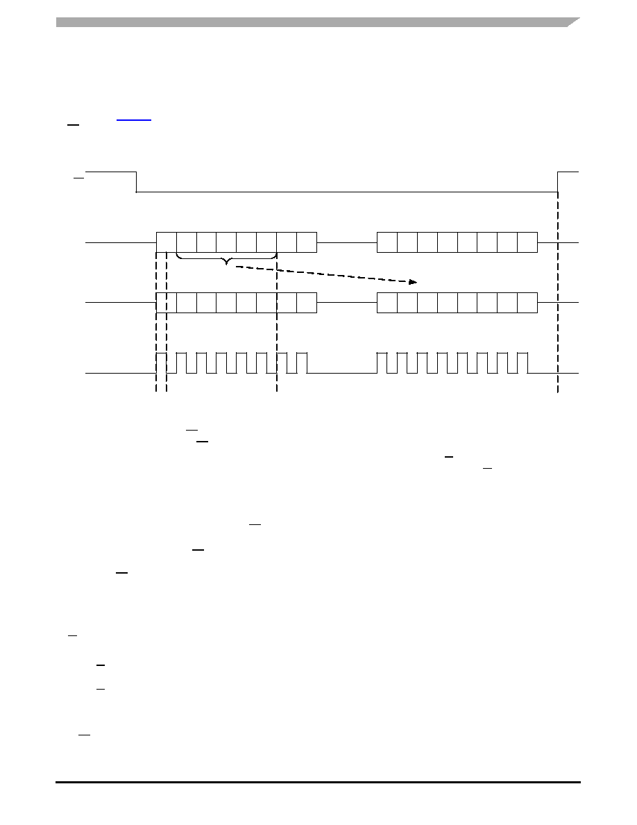
Figure 9. SPI Protocol
During the inactive phase of SS, the new data transfer is
prepared. The falling edge on the SS line indicates the start
of a new data transfer and puts MISO in the low-impedance
mode. The first valid data are moved to MISO with the rising
edge of SPSCK.
The MISO output changes data on a rising edge of
SPSCK. The MOSI input is sampled on a falling edge of
SPSCK. The data transfer is only valid if exactly 16 sample
clock edges are present in the active phase of SS.
After a write operation, the transmitted data is latched into
the register by the rising edge of SS. Register read data is
internally latched into the SPI at the time when the parity bit
is transferred. SS HIGH forces MISO to high impedance.
A4:A0
Contains the address of the desired register.
R/W
Contains information about a read or a write operation.
If R/W = 1, the second byte of master contains no valid
information, slave just transmits back register data.
If R/W = 0, the master sends data to be written in the
second byte, slave sends concurrently contents of
selected register prior to write operation, write data is
latched in the SMARTMOS register on rising edge of
SS
.
PARITY P
The parity bit is equal to 0 if the number of 1 bits is an even
number contained within R/W, A4:A0. If the number of 1 bits
is odd, P equals 1. For example, if R/W = 1, A4:A0 = 00001,
then P equals 0.
The parity bit is only evaluated during a write operation.
BIT X
Not used.
MASTER DATA BYTE
Contains data to be written or no valid data during a read
operation.
SLAVE STATUS BYTE
Contains the contents of the System Status Register ($0c)
independent of whether it is a write or read operation or which
register was selected.
SLAVE DATA BYTE
Contains the contents of selected register. During a write
operation it includes the register content prior to a write
operation.
S7
S6
S5
S4
S3
S2
S1
S0
R/W
A4
A3
A2
A1
A0
P
X
D7
D6
D5
D4
D3
D2
D1
D0
D7
D6
D5
D4
D3
D2
D1
D0
System Status Register
Read/Write, Address, Parity
Data (Register write)
Data (Register read)
Rising edge of SPSCK
Change MISO/MOSI
Output
Falling edge of SPSCK
Sample MISO/MOSI
Input
Slave latch
register address
Slave latch
data
SS
MOSI
MISO
SPSCK
相关PDF资料 |
PDF描述 |
|---|---|
| MAX6440UTLQZD7+T | IC BATTERY MON SNGL SOT23-6 |
| UVR2F2R2MPD | CAP ALUM 2.2UF 315V 20% RADIAL |
| MAX6440UTLQYD7+T | IC BATTERY MON SNGL SOT23-6 |
| MAX6440UTKSYD7+T | IC BATTERY MON SNGL SOT23-6 |
| MAX6440UTMRSD3+T | IC BATTERY MON SNGL SOT23-6 |
相关代理商/技术参数 |
参数描述 |
|---|---|
| KIT-910 | 制造商:Anderson Power Products (APP) 功能描述:KIT |
| KIT912F634EVME | 功能描述:开发板和工具包 - S08 / S12 INTEGRATED DUAL L/H SWIT RoHS:否 产品:Development Kits 工具用于评估:MC9S12G128 核心:S12 接口类型:CAN, LIN, RS-232, USB 工作电源电压:5 V 制造商:Freescale Semiconductor |
| KIT912H634EVME | 功能描述:开发板和工具包 - S08 / S12 DUAL LOW&HIDE SWITCH EVB RoHS:否 产品:Development Kits 工具用于评估:MC9S12G128 核心:S12 接口类型:CAN, LIN, RS-232, USB 工作电源电压:5 V 制造商:Freescale Semiconductor |
| KIT912J637EVME | 功能描述:电源管理IC开发工具 BATTERY SENSOR 912J637 RoHS:否 制造商:Maxim Integrated 产品:Evaluation Kits 类型:Battery Management 工具用于评估:MAX17710GB 输入电压: 输出电压:1.8 V |
| KIT912S812ECUEVM | 功能描述:电源管理IC开发工具 Single Cylinder S12XS E RoHS:否 制造商:Maxim Integrated 产品:Evaluation Kits 类型:Battery Management 工具用于评估:MAX17710GB 输入电压: 输出电压:1.8 V |
发布紧急采购,3分钟左右您将得到回复。