- 您现在的位置:买卖IC网 > PDF目录3987 > KMPC8555EPXAQF (Freescale Semiconductor)IC MPU POWERQUICC III 783-FCPBGA PDF资料下载
参数资料
| 型号: | KMPC8555EPXAQF |
| 厂商: | Freescale Semiconductor |
| 文件页数: | 26/88页 |
| 文件大小: | 0K |
| 描述: | IC MPU POWERQUICC III 783-FCPBGA |
| 标准包装: | 2 |
| 系列: | MPC85xx |
| 处理器类型: | 32-位 MPC85xx PowerQUICC III |
| 速度: | 1.0GHz |
| 电压: | 1.3V |
| 安装类型: | 表面贴装 |
| 封装/外壳: | 783-BBGA,FCBGA |
| 供应商设备封装: | 783-FCPBGA(29x29) |
| 包装: | 托盘 |
第1页第2页第3页第4页第5页第6页第7页第8页第9页第10页第11页第12页第13页第14页第15页第16页第17页第18页第19页第20页第21页第22页第23页第24页第25页当前第26页第27页第28页第29页第30页第31页第32页第33页第34页第35页第36页第37页第38页第39页第40页第41页第42页第43页第44页第45页第46页第47页第48页第49页第50页第51页第52页第53页第54页第55页第56页第57页第58页第59页第60页第61页第62页第63页第64页第65页第66页第67页第68页第69页第70页第71页第72页第73页第74页第75页第76页第77页第78页第79页第80页第81页第82页第83页第84页第85页第86页第87页第88页
MPC8555E PowerQUICC III Integrated Communications Processor Hardware Specification, Rev. 4.2
32
Freescale Semiconductor
Ethernet: Three-Speed, MII Management
8.3.2
MII Management AC Electrical Specifications
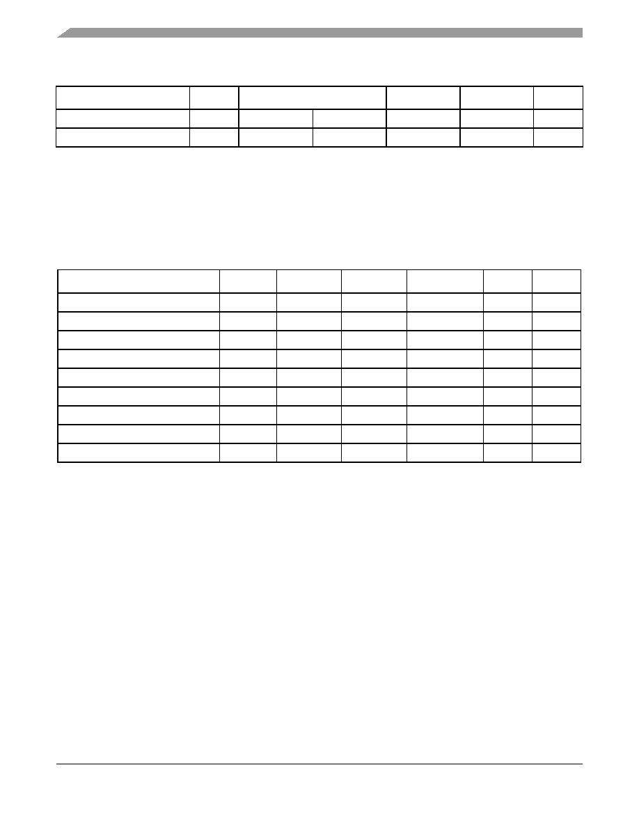
Table 28 provides the MII management AC timing specifications.
Input high current
IIH
LVDD = Max
VIN
1 = 2.1 V
—
40
μA
Input low current
IIL
LVDD = Max
VIN = 0.5 V
–600
—
μA
Note:
1. Note that the symbol VIN, in this case, represents the OVIN symbol referenced in Table 1 and Table 2.
Table 28. MII Management AC Timing Specifications
At recommended operating conditions with LVDD is 3.3 V ± 5%.
Parameter/Condition
Symbol 1
Min
Typ
Max
Unit
Notes
MDC frequency
fMDC
0.893
—
10.4
MHz
2
MDC period
tMDC
96
—
1120
ns
MDC clock pulse width high
tMDCH
32
—
ns
MDC to MDIO valid
tMDKHDV
2*[1/(fccb_clk/8)]
ns
3
MDC to MDIO delay
tMDKHDX
10
—
2*[1/(fccb_clk/8)]
ns
3
MDIO to MDC setup time
tMDDVKH
5—
—
ns
MDIO to MDC hold time
tMDDXKH
0—
—
ns
MDC rise time
tMDCR
—
10
ns
MDC fall time
tMDHF
—
10
ns
Notes:
1. The symbols used for timing specifications herein follow the pattern of t(first two letters of functional block)(signal)(state)
(reference)(state) for inputs and t(first two letters of functional block)(reference)(state)(signal)(state) for outputs. For example, tMDKHDX
symbolizes management data timing (MD) for the time tMDC from clock reference (K) high (H) until data outputs (D) are
invalid (X) or data hold time. Also, tMDDVKH symbolizes management data timing (MD) with respect to the time data input
signals (D) reach the valid state (V) relative to the tMDC clock reference (K) going to the high (H) state or setup time. For
rise and fall times, the latter convention is used with the appropriate letter: R (rise) or F (fall).
2. This parameter is dependent on the system clock speed (that is, for a system clock of 267 MHz, the delay is 70 ns and for
a system clock of 333 MHz, the delay is 58 ns).
3. This parameter is dependent on the CCB clock speed (that is, for a CCB clock of 267 MHz, the delay is 60 ns and for a
CCB clock of 333 MHz, the delay is 48 ns).
4. Guaranteed by design.
Table 27. MII Management DC Electrical Characteristics (continued)
Parameter
Symbol
Conditions
Min
Max
Unit
相关PDF资料 |
PDF描述 |
|---|---|
| FMC49DRES-S734 | CONN EDGECARD 98POS .100 EYELET |
| FMC65DRAS | CONN EDGECARD 130PS R/A .100 SLD |
| XCS20-3PQ208I | IC FPGA 5V I-TEMP 208-PQFP |
| XCS10XL-4VQ100I | IC FPGA 3.3V I-TEMP 100-VQFP |
| KMPC860DEVR80D4 | IC MPU POWERQUICC 80MHZ 357-PBGA |
相关代理商/技术参数 |
参数描述 |
|---|---|
| KMPC8555EVTALF | 功能描述:微处理器 - MPU PQ 37 LITE 8555E RoHS:否 制造商:Atmel 处理器系列:SAMA5D31 核心:ARM Cortex A5 数据总线宽度:32 bit 最大时钟频率:536 MHz 程序存储器大小:32 KB 数据 RAM 大小:128 KB 接口类型:CAN, Ethernet, LIN, SPI,TWI, UART, USB 工作电源电压:1.8 V to 3.3 V 最大工作温度:+ 85 C 安装风格:SMD/SMT 封装 / 箱体:FBGA-324 |
| KMPC8555EVTAPF | 功能描述:微处理器 - MPU PQ 37 LITE 8555E RoHS:否 制造商:Atmel 处理器系列:SAMA5D31 核心:ARM Cortex A5 数据总线宽度:32 bit 最大时钟频率:536 MHz 程序存储器大小:32 KB 数据 RAM 大小:128 KB 接口类型:CAN, Ethernet, LIN, SPI,TWI, UART, USB 工作电源电压:1.8 V to 3.3 V 最大工作温度:+ 85 C 安装风格:SMD/SMT 封装 / 箱体:FBGA-324 |
| KMPC8555EVTAQF | 功能描述:微处理器 - MPU PQ 37 LITE 8555E RoHS:否 制造商:Atmel 处理器系列:SAMA5D31 核心:ARM Cortex A5 数据总线宽度:32 bit 最大时钟频率:536 MHz 程序存储器大小:32 KB 数据 RAM 大小:128 KB 接口类型:CAN, Ethernet, LIN, SPI,TWI, UART, USB 工作电源电压:1.8 V to 3.3 V 最大工作温度:+ 85 C 安装风格:SMD/SMT 封装 / 箱体:FBGA-324 |
| KMPC8555PXALF | 功能描述:微处理器 - MPU PQ 37 LITE 8555 RoHS:否 制造商:Atmel 处理器系列:SAMA5D31 核心:ARM Cortex A5 数据总线宽度:32 bit 最大时钟频率:536 MHz 程序存储器大小:32 KB 数据 RAM 大小:128 KB 接口类型:CAN, Ethernet, LIN, SPI,TWI, UART, USB 工作电源电压:1.8 V to 3.3 V 最大工作温度:+ 85 C 安装风格:SMD/SMT 封装 / 箱体:FBGA-324 |
| KMPC8555PXAPF | 功能描述:微处理器 - MPU PQ 37 LITE 8555 RoHS:否 制造商:Atmel 处理器系列:SAMA5D31 核心:ARM Cortex A5 数据总线宽度:32 bit 最大时钟频率:536 MHz 程序存储器大小:32 KB 数据 RAM 大小:128 KB 接口类型:CAN, Ethernet, LIN, SPI,TWI, UART, USB 工作电源电压:1.8 V to 3.3 V 最大工作温度:+ 85 C 安装风格:SMD/SMT 封装 / 箱体:FBGA-324 |
发布紧急采购,3分钟左右您将得到回复。