- 您现在的位置:买卖IC网 > PDF目录19715 > LC5512MB-45FN256C (Lattice Semiconductor Corporation)IC CPLD 512MACROCELLS 256FPBGA PDF资料下载
参数资料
| 型号: | LC5512MB-45FN256C |
| 厂商: | Lattice Semiconductor Corporation |
| 文件页数: | 25/99页 |
| 文件大小: | 0K |
| 描述: | IC CPLD 512MACROCELLS 256FPBGA |
| 标准包装: | 90 |
| 系列: | ispXPLD® 5000MB |
| 可编程类型: | 系统内可编程 |
| 最大延迟时间 tpd(1): | 4.5ns |
| 电压电源 - 内部: | 2.3 V ~ 2.7 V |
| 逻辑元件/逻辑块数目: | 16 |
| 宏单元数: | 512 |
| 输入/输出数: | 193 |
| 工作温度: | 0°C ~ 90°C |
| 安装类型: | 表面贴装 |
| 封装/外壳: | 256-BGA |
| 供应商设备封装: | 256-FPBGA(17x17) |
| 包装: | 托盘 |
第1页第2页第3页第4页第5页第6页第7页第8页第9页第10页第11页第12页第13页第14页第15页第16页第17页第18页第19页第20页第21页第22页第23页第24页当前第25页第26页第27页第28页第29页第30页第31页第32页第33页第34页第35页第36页第37页第38页第39页第40页第41页第42页第43页第44页第45页第46页第47页第48页第49页第50页第51页第52页第53页第54页第55页第56页第57页第58页第59页第60页第61页第62页第63页第64页第65页第66页第67页第68页第69页第70页第71页第72页第73页第74页第75页第76页第77页第78页第79页第80页第81页第82页第83页第84页第85页第86页第87页第88页第89页第90页第91页第92页第93页第94页第95页第96页第97页第98页第99页
Lattice Semiconductor
ispXPLD 5000MX Family Data Sheet
27
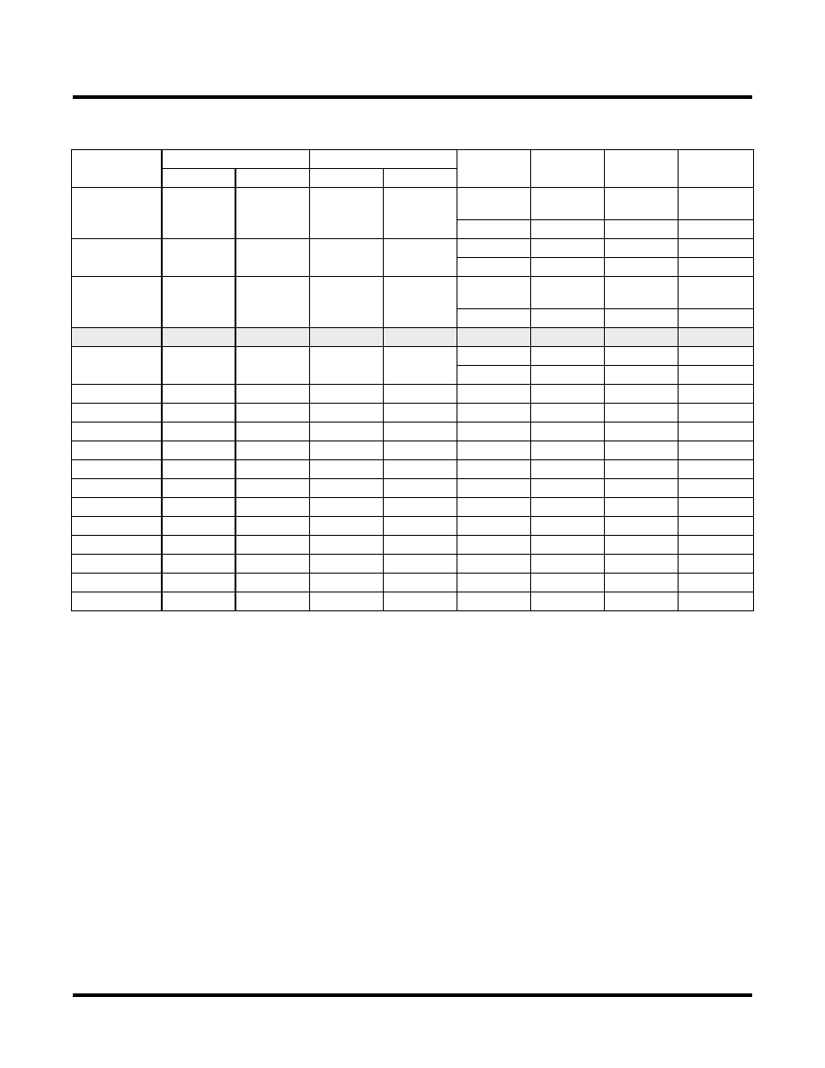
sysIO Single Ended DC Electrical Characteristics
Over Recommended Operating Conditions
Input/Output
Standard
VIL
VIH
VOL
Max (V)
VOH
Min (V)
IOL
2
(mA)
IOH
2
(mA)
Min (V)
Max (V)
Min (V)
Max (V)
LVCMOS 3.3
-0.3
0.8
2.0
5.5
0.4
2.4
20, 16, 12,
8, 5.33, 4
-20, -16, -12,
-8, -5.33, -4
0.2
VCCO - 0.2
0.1
-0.1
LVTTL
-0.3
0.8
2.0
5.5
0.4
2.4
4
-4
0.2
VCCO - 0.2
0.1
-0.1
LVCMOS 2.5
-0.3
0.7
1.7
3.6
0.4
VCCO - 0.4
16, 12, 8,
5.33, 4
-16, -12, -8,
-5.33, -4
0.2
VCCO - 0.2
0.1
-0.1
LVCMOS 1.8
1, 3
-0.3
0.68
1.07
3.6
0.4
VCCO - 0.4
8
-8
LVCMOS 1.8
3
-0.3
0.68
1.07
3.6
0.4
VCCO -0.4
12, 5.33, 4 -12, -5.33, -4
0.2
VCCO - 0.2
0.1
-0.1
PCI 3.3
4
-0.3
1.08
1.5
3.6
0.1 VCCO
0.9 VCCO
1.5
-0.5
AGP-1X
4
-0.3
1.08
1.5
3.6
0.1 VCCO
0.9 VCCO
1.5
-0.5
SSTL3 class I
-0.3
VREF - 0.2
VREF + 0.2
3.6
0.7
VCCO - 1.1
8
-8
SSTL3 class II
-0.3
VREF - 0.2
VREF + 0.2
3.6
0.5
VCCO - 0.9
16
-16
SSTL2 class I
-0.3
VREF - 0.18 VREF + 0.18
3.6
0.54
VCCO - 0.62
7.6
-7.6
SSTL2 class II
-0.3
VREF - 0.18 VREF + 0.18
3.6
0.35
VCCO - 0.43
15.2
-15.2
CTT 3.3
-0.3
VREF - 0.2
VREF + 0.2
3.6
VREF - 0.4
VREF + 0.4
8
-8
CTT 2.5
-0.3
VREF - 0.3
VREF + 0.2
3.6
VREF - 0.4
VREF + 0.4
8
-8
HSTL class I
-0.3
VREF - 0.1
VREF + 0.1
3.6
0.4
VCCO - 0.4
8
-8
HSTL class III
-0.3
VREF - 0.2
VREF + 0.1
3.6
0.4
VCCO - 0.4
24
-8
HSTL class IV
-0.3
VREF - 0.3
VREF + 0.1
3.6
0.4
VCCO - 0.4
48
-8
GTL+
-0.3
VREF - 0.2
VREF + 0.2
3.6
0.6
n/a
36
n/a
1. Software default setting.
2. The average DC current drawn by I/Os between adjacent bank GND connections, or between the last GND in an I/O bank and the end of the
I/O bank, as shown in the logic signals connection table, shall not exceed n*8mA. Where n is the number of I/Os between bank GND con-
nections or between the last GND in a bank and the end of a bank.
3. For 1.8V devices (ispXPLD 5000MC) these specifications are VIL = 0.35 * VCC and VIH = 0.65 * VCC.
4. For 1.8V devices (ispXPLD 5000MC) these specifications are VIL = 0.3 * VCC * 3.3/1.8, VIH = 0.5 * VCC * 3.3/1.8.
SELECT
DEVICES
DISCONTINUED
相关PDF资料 |
PDF描述 |
|---|---|
| 180-015-102L011 | CONN DB15 MALE HD SOLDER CUP TIN |
| EMA43DRMD | CONN EDGECARD 86POS .125 SQ WW |
| 180-015-103L021 | CONN DB15 MALE HD SLD CUP NICKEL |
| MIC39150-1.8BT | IC REG LDO 1.8V 1.5A TO-220 |
| TOP247FN | IC OFFLINE SWIT UVLO HV TO262 |
相关代理商/技术参数 |
参数描述 |
|---|---|
| LC5512MB-45FN256I | 制造商:LATTICE 制造商全称:Lattice Semiconductor 功能描述:3.3V, 2.5V and 1.8V In-System Programmable eXpanded Programmable Logic Device XPLD⑩ Family |
| LC5512MB-45FN484C | 功能描述:CPLD - 复杂可编程逻辑器件 PROGRAM EXPANDED LOG RoHS:否 制造商:Lattice 系列: 存储类型:EEPROM 大电池数量:128 最大工作频率:333 MHz 延迟时间:2.7 ns 可编程输入/输出端数量:64 工作电源电压:3.3 V 最大工作温度:+ 90 C 最小工作温度:0 C 封装 / 箱体:TQFP-100 |
| LC5512MB-45FN484I | 制造商:LATTICE 制造商全称:Lattice Semiconductor 功能描述:3.3V, 2.5V and 1.8V In-System Programmable eXpanded Programmable Logic Device XPLD⑩ Family |
| LC5512MB-45FN672C | 制造商:LATTICE 制造商全称:Lattice Semiconductor 功能描述:3.3V, 2.5V and 1.8V In-System Programmable eXpanded Programmable Logic Device XPLD⑩ Family |
| LC5512MB-45FN672I | 制造商:LATTICE 制造商全称:Lattice Semiconductor 功能描述:3.3V, 2.5V and 1.8V In-System Programmable eXpanded Programmable Logic Device XPLD⑩ Family |
发布紧急采购,3分钟左右您将得到回复。