- 您现在的位置:买卖IC网 > PDF目录19715 > LC5512MB-45FN256C (Lattice Semiconductor Corporation)IC CPLD 512MACROCELLS 256FPBGA PDF资料下载
参数资料
| 型号: | LC5512MB-45FN256C |
| 厂商: | Lattice Semiconductor Corporation |
| 文件页数: | 42/99页 |
| 文件大小: | 0K |
| 描述: | IC CPLD 512MACROCELLS 256FPBGA |
| 标准包装: | 90 |
| 系列: | ispXPLD® 5000MB |
| 可编程类型: | 系统内可编程 |
| 最大延迟时间 tpd(1): | 4.5ns |
| 电压电源 - 内部: | 2.3 V ~ 2.7 V |
| 逻辑元件/逻辑块数目: | 16 |
| 宏单元数: | 512 |
| 输入/输出数: | 193 |
| 工作温度: | 0°C ~ 90°C |
| 安装类型: | 表面贴装 |
| 封装/外壳: | 256-BGA |
| 供应商设备封装: | 256-FPBGA(17x17) |
| 包装: | 托盘 |
第1页第2页第3页第4页第5页第6页第7页第8页第9页第10页第11页第12页第13页第14页第15页第16页第17页第18页第19页第20页第21页第22页第23页第24页第25页第26页第27页第28页第29页第30页第31页第32页第33页第34页第35页第36页第37页第38页第39页第40页第41页当前第42页第43页第44页第45页第46页第47页第48页第49页第50页第51页第52页第53页第54页第55页第56页第57页第58页第59页第60页第61页第62页第63页第64页第65页第66页第67页第68页第69页第70页第71页第72页第73页第74页第75页第76页第77页第78页第79页第80页第81页第82页第83页第84页第85页第86页第87页第88页第89页第90页第91页第92页第93页第94页第95页第96页第97页第98页第99页
Lattice Semiconductor
ispXPLD 5000MX Family Data Sheet
43
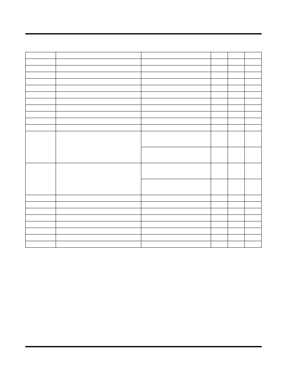
sysCLOCK PLL Timing
Over Recommended Operating Conditions
Symbol
Parameter
Conditions
Min
Max
Units
tPWH
Input clock, high time
80% to 80%
1.2
—
ns
tPWL
Input clock, low time
20% to 20%
1.2
—
ns
tR, tF
Input Clock, rise and fall time
20% to 80%
—
3.0
ns
tINSTB
Input clock stability, cycle to cycle (peak)
—
+/- 250
ps
fMDIVIN
M Divider input, frequency range
10
320
MHz
fMDIVOUT
M Divider output, frequency range
10
320
MHz
fNDIVIN
N Divider input, frequency range
10
320
MHz
fNDIVOUT
N Divider output, frequency range
10
320
MHz
fVDIVIN
V Divider input, frequency range
100
400
MHz
fVDIVOUT
V Divider output, frequency range
10
320
MHz
tOUTDUTY
Output clock, duty cycle
40
60
%
tJIT(CC)
Output clock, cycle to cycle jitter (peak)
Clean reference.
10 MHz < fMDIVOUT < 20 MHz or
100MHz < fVDIVIN < 160 MHz
1
—
+/- 250
ps
Clean reference.
20 MHz < fMDIVOUT < 320 MHz and
160MHz < fVDIVIN < 320 MHz
1
—
+/- 150
ps
TJIT(PERIOD)
2
Output clock, period jitter (peak)
Clean reference.
10 MHz < fMDIVOUT < 20 MHz or
100MHz < fVDIVIN < 160 MHz
1
—
+/- 300
ps
Clean reference.
20 MHz < fMDIVOUT < 320 MHz and
160MHz < fVDIVIN < 320 MHz
1
—
+/- 150
ps
tCLK_OUT_DLY
Input clock to CLK_OUT delay
Internal feedback
—
3.0
ns
tPHASE
Input clock to external feedback delta
External feedback
—
600
ps
tLOCK
Time to acquire phase lock after input stable
—
25
us
tPLL_DELAY
Delay increment (Lead/Lag)
Typical = +/- 250ps
+/- 120 +/- 550
ps
tRANGE
Total output delay range (lead/lag)
+/- 0.84 +/- 3.85
ns
tPLL_RSTW
Minimum reset pulse width
—
1.8
ns
tCLK_IN
3
Global clock input delay
—
1.0
ns
tPLL_SEC_DELAY Secondary PLL output delay (tPLL_DELAY)—
1.5
ns
1. This condition assures that the output phase jitter will remain within specification.
2. Accumulated jitter measured over 10,000 waveform samples.
3. Internal timing for reference only.
SELECT
DEVICES
DISCONTINUED
相关PDF资料 |
PDF描述 |
|---|---|
| 180-015-102L011 | CONN DB15 MALE HD SOLDER CUP TIN |
| EMA43DRMD | CONN EDGECARD 86POS .125 SQ WW |
| 180-015-103L021 | CONN DB15 MALE HD SLD CUP NICKEL |
| MIC39150-1.8BT | IC REG LDO 1.8V 1.5A TO-220 |
| TOP247FN | IC OFFLINE SWIT UVLO HV TO262 |
相关代理商/技术参数 |
参数描述 |
|---|---|
| LC5512MB-45FN256I | 制造商:LATTICE 制造商全称:Lattice Semiconductor 功能描述:3.3V, 2.5V and 1.8V In-System Programmable eXpanded Programmable Logic Device XPLD⑩ Family |
| LC5512MB-45FN484C | 功能描述:CPLD - 复杂可编程逻辑器件 PROGRAM EXPANDED LOG RoHS:否 制造商:Lattice 系列: 存储类型:EEPROM 大电池数量:128 最大工作频率:333 MHz 延迟时间:2.7 ns 可编程输入/输出端数量:64 工作电源电压:3.3 V 最大工作温度:+ 90 C 最小工作温度:0 C 封装 / 箱体:TQFP-100 |
| LC5512MB-45FN484I | 制造商:LATTICE 制造商全称:Lattice Semiconductor 功能描述:3.3V, 2.5V and 1.8V In-System Programmable eXpanded Programmable Logic Device XPLD⑩ Family |
| LC5512MB-45FN672C | 制造商:LATTICE 制造商全称:Lattice Semiconductor 功能描述:3.3V, 2.5V and 1.8V In-System Programmable eXpanded Programmable Logic Device XPLD⑩ Family |
| LC5512MB-45FN672I | 制造商:LATTICE 制造商全称:Lattice Semiconductor 功能描述:3.3V, 2.5V and 1.8V In-System Programmable eXpanded Programmable Logic Device XPLD⑩ Family |
发布紧急采购,3分钟左右您将得到回复。