- 您现在的位置:买卖IC网 > PDF目录177665 > LC5512MC-75QN208I (LATTICE SEMICONDUCTOR CORP) PDF资料下载
参数资料
| 型号: | LC5512MC-75QN208I |
| 厂商: | LATTICE SEMICONDUCTOR CORP |
| 元件分类: | PLD |
| 中文描述: | EE PLD, 9.5 ns, PQFP208 |
| 封装: | LEAD FREE, PLASTIC, QFP-208 |
| 文件页数: | 23/95页 |
| 文件大小: | 923K |
| 代理商: | LC5512MC-75QN208I |
第1页第2页第3页第4页第5页第6页第7页第8页第9页第10页第11页第12页第13页第14页第15页第16页第17页第18页第19页第20页第21页第22页当前第23页第24页第25页第26页第27页第28页第29页第30页第31页第32页第33页第34页第35页第36页第37页第38页第39页第40页第41页第42页第43页第44页第45页第46页第47页第48页第49页第50页第51页第52页第53页第54页第55页第56页第57页第58页第59页第60页第61页第62页第63页第64页第65页第66页第67页第68页第69页第70页第71页第72页第73页第74页第75页第76页第77页第78页第79页第80页第81页第82页第83页第84页第85页第86页第87页第88页第89页第90页第91页第92页第93页第94页第95页
Lattice Semiconductor
ispXPLD 5000MX Family Data Sheet
3
5000MX. Incoming signals may connect to the global routing pool or the registers in the MFBs. An Output Sharing
Array (OSA) increases the number of I/O available to each MFB, allowing a complete function high-performance
access to the I/O. There are four clock pins that drive four global clock nets within the device. Two sysCLOCK PLLs
are provided to allow the synthesis of new clocks and control of clock skews.
Multi-Function Block (MFB)
Each MFB in the ispXPLD 5000MX architecture can be configured in one of the six following modes. This provides
a flexible approach to implementing logic and memory that allows the designer to achieve the mix of functions that
are required for a particular design, maximizing resource utilization. The six modes supported by the MFB are:
SuperWIDE Logic Mode
True Dual-port SRAM Mode
Pseudo Dual-port SRAM Mode
Single-port SRAM Mode
FIFO Mode
Ternary CAM Mode
The MFB consists of a multi-function array and associated routing. Depending on the chosen functions the multi-
function array uses up to 68 inputs from the GRP and the four global clock and reset signals. The array outputs
data along with certain control functions to the macrocells. Output signals can be routed internally for use else-
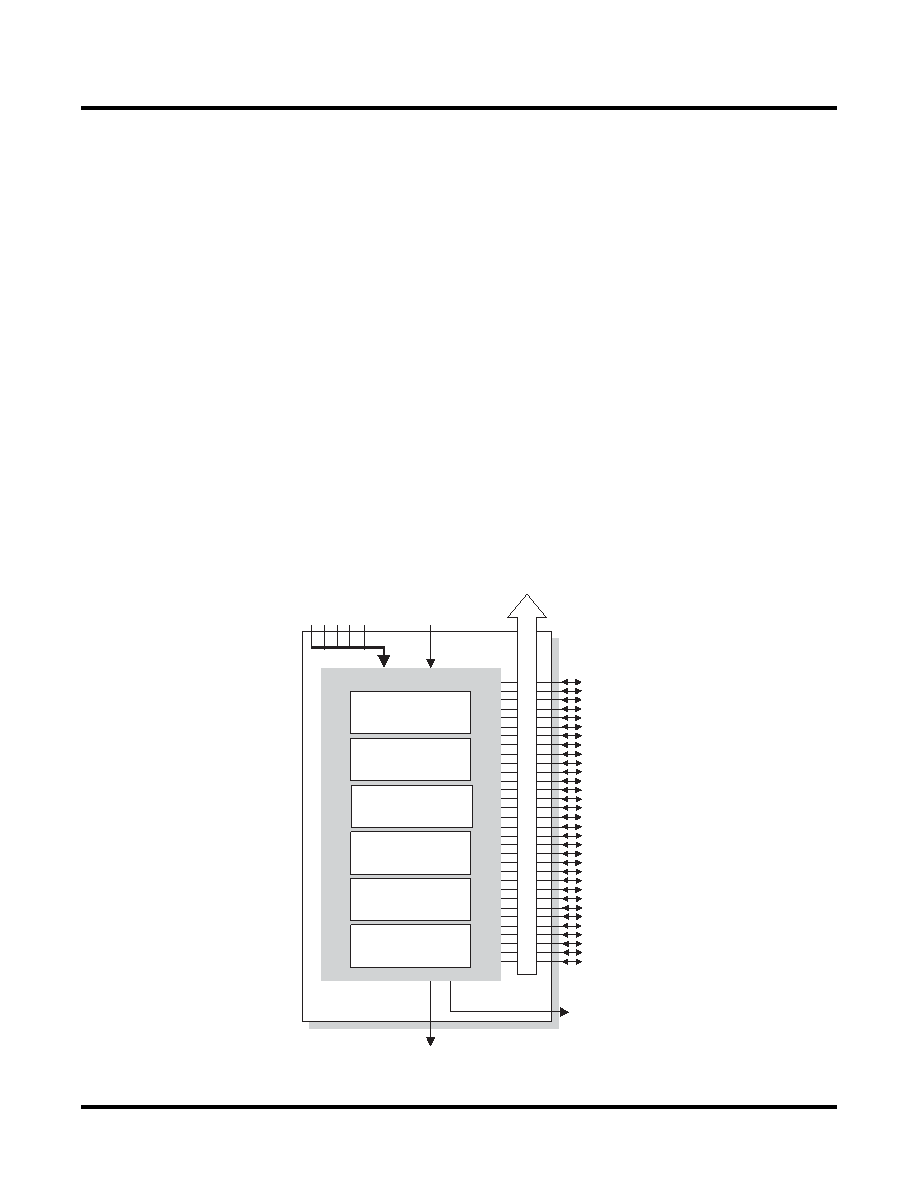
where in the device and to the sysIO banks for output. Figure 2 shows the block diagram of the MFB. The various
configurations are described in more detail in the following sections.
Figure 2. MFB Block Diagram
To Routing
Reset
CLK0
CLK3
CLK1
CLK2
PTOE
Sharing
To
I/O
via
OSA
Cascade
In
Cascade Out
Multifunction Array
True Dual Port
RAM
(8,192 bit)
Pseudo Dual
Port RAM
(16,384 bit)
Single Port
RAM
(16,384 bit)
FIFO
(16,384 bit)
Ternary CAM
(128*48)
Logic
(68 Input * 164 Product
Term Array, 32 MC)
32
Feedback
Signals
相关PDF资料 |
PDF描述 |
|---|---|
| LC51024MC-75FN484C | |
| LC51024MC-52FN484C | |
| LC5768MC-5FN256C | |
| LC51024MC-75FN672I | |
| LC51024MB-75FN484C | |
相关代理商/技术参数 |
参数描述 |
|---|---|
| LC5512M-PAC-EV | 功能描述:可编程逻辑 IC 开发工具 Eval Board for XPLD5512 PAC1208 RoHS:否 制造商:Altera Corporation 产品:Development Kits 类型:FPGA 工具用于评估:5CEFA7F3 接口类型: 工作电源电压: |
| LC5512MV-45F208C | 制造商:LATTICE 制造商全称:Lattice Semiconductor 功能描述:3.3V, 2.5V and 1.8V In-System Programmable eXpanded Programmable Logic Device XPLD⑩ Family |
| LC5512MV-45F208I | 制造商:LATTICE 制造商全称:Lattice Semiconductor 功能描述:3.3V, 2.5V and 1.8V In-System Programmable eXpanded Programmable Logic Device XPLD⑩ Family |
| LC5512MV-45F256C | 功能描述:CPLD - 复杂可编程逻辑器件 3.3V 193 I/O RoHS:否 制造商:Lattice 系列: 存储类型:EEPROM 大电池数量:128 最大工作频率:333 MHz 延迟时间:2.7 ns 可编程输入/输出端数量:64 工作电源电压:3.3 V 最大工作温度:+ 90 C 最小工作温度:0 C 封装 / 箱体:TQFP-100 |
| LC5512MV-45F256I | 制造商:LATTICE 制造商全称:Lattice Semiconductor 功能描述:3.3V, 2.5V and 1.8V In-System Programmable eXpanded Programmable Logic Device XPLD⑩ Family |
发布紧急采购,3分钟左右您将得到回复。