- 您现在的位置:买卖IC网 > PDF目录19710 > LC5512MV-45F484C (Lattice Semiconductor Corporation)IC XPLD 512MC 4.5NS 484FPBGA PDF资料下载
参数资料
| 型号: | LC5512MV-45F484C |
| 厂商: | Lattice Semiconductor Corporation |
| 文件页数: | 51/99页 |
| 文件大小: | 0K |
| 描述: | IC XPLD 512MC 4.5NS 484FPBGA |
| 标准包装: | 60 |
| 系列: | ispXPLD® 5000MV |
| 可编程类型: | 系统内可编程 |
| 最大延迟时间 tpd(1): | 4.5ns |
| 电压电源 - 内部: | 3 V ~ 3.6 V |
| 逻辑元件/逻辑块数目: | 16 |
| 宏单元数: | 512 |
| 输入/输出数: | 253 |
| 工作温度: | 0°C ~ 90°C |
| 安装类型: | 表面贴装 |
| 封装/外壳: | 484-BBGA |
| 供应商设备封装: | 484-FPBGA(23x23) |
| 包装: | 托盘 |
第1页第2页第3页第4页第5页第6页第7页第8页第9页第10页第11页第12页第13页第14页第15页第16页第17页第18页第19页第20页第21页第22页第23页第24页第25页第26页第27页第28页第29页第30页第31页第32页第33页第34页第35页第36页第37页第38页第39页第40页第41页第42页第43页第44页第45页第46页第47页第48页第49页第50页当前第51页第52页第53页第54页第55页第56页第57页第58页第59页第60页第61页第62页第63页第64页第65页第66页第67页第68页第69页第70页第71页第72页第73页第74页第75页第76页第77页第78页第79页第80页第81页第82页第83页第84页第85页第86页第87页第88页第89页第90页第91页第92页第93页第94页第95页第96页第97页第98页第99页
Lattice Semiconductor
ispXPLD 5000MX Family Data Sheet
51
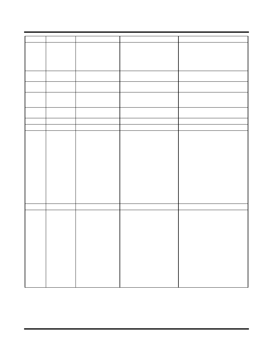
Signals
208 PQFP
4
256 fpBGA
3, 5
484 fpBGA, 5
3
672 fpBGA
3, 5
VCC
10, 49, 76, 114,
153, 180
D4, D13, F6, F11, L6,
L11, N4, N13
A17, A6, AA2, AA21, AB17,
AB6, B2, B21, D19, D4, F1,
F22, G10, G11, G12, G13, K16,
K7, L16, L7, M16, M7, T10,
T11, T12, T13, T14, T9, U1,
U22, W19, W4
AA21, AA6, F21, F6, G20, G7, J13,
J14, K13, K14, L13, L14, M13, M14,
N10, N11, N12, N15, N16, N17, N18,
N9, P10, P11, P12, P15, P16, P17,
P18, P9, R13, R14, T13, T14, U13,
U14, V13, V14, Y20, Y7
VCCO0
5, 17, 189, 204 A1, F7, G6
B9, C3, G8, G9, H7, J2, J7, P4
H10, H11, H8, H9, J8, J9, K8, L8, M8,
N8
VCCO1
42, 57, 72
K6, L7, T1
AA9, R7, T3, T8, Y3
P8, R8, T8, U8, V8, V9, W10, W11,
W8, W9
VCCO2
85, 100, 107,
121
K11, L10, T16
AA14, R16, T15, T20, Y20
P19, R19, T19, U19, V18, V19, W12,
W13, W14, W15, W16, W17, W18,
W19
VCCO3
146, 161, 176
A16, F10, G11
B14, C20, G14, G15, H16, J16,
J21, P19
H12, H13, H14, H15, H16, H17, H18,
H19, J18, J19, K19, L19, M19, N19
VCCP
136
J16
M22
N25
VCCJ
27
J1
M1
N4
GND
15, 29, 44, 81,
119, 148, 185,
7, 19, 191, 205,
40, 56, 70, 87,
101, 109, 123,
144, 160, 174
K1, C3, C14, E5, E12,
G7, G8, G9, G10, H7,
H8, H9, H10, J7, J8, J9,
J10, K7, K8, K9, K10,
M5, M12, P3
N1, A1, A2, A21, A22, AA1,
AA22, AB1, AB22, B1, B22,
C15, C8, D11, D12, E18, E5,
F17, F6, G16, G7, H10, H11,
H12, H13, H14, H15, H20, H3,
H8, H9, J10, J11, J12, J13, J14,
J15, J8, J9, K10, K11, K12,
K13, K14, K15, K8, K9, L10,
L11, L12, L13, L14, L15, L19,
L4, L8, L9, M10, M11, M12,
M13, M14, M19, M4, M9, N10,
N11, N12, N13, N14, N9, P10,
P11, P12, P13, P14, P9, R10,
R11, R12, R13, R14, R15, R8,
R9, T16, T7, W11, W12, Y15,
Y8
A11, A16, A2, A25, AE1, AE2, AE25,
AE26, AF11, AF16, AF2, AF25, B1,
B2, B25, B26, J10, J11, J12, J15, J16,
J17, K10, K11, K12, K15, K16, K17,
K18, K9, L1, L10, L11, L12, L15, L16,
L17, L18, L26, L9, M10, M11, M12,
M15, M16, M17, M18, M9, N13, N14,
P13, P14, R10, R11, R12, R15, R16,
R17, R18, R9, T1, T10, T11, T12,
T15, T16, T17, T18, T26, T9, U10,
U11, U12, U15, U16, U17, U18, U9,
V10, V11, V12, V15, V16, V17
GNDP
134
K16
N22
P26
NC
2
—
5256MX: A2, A11, A12,
A15, B2, B12, B15,
B16, C4, C12, C15,
C16, D1, D11, D14,
D15, D16, E1, E4, E10,
E11, E13, E14, F4, F5,
F12, F13, L1, L4, M3,
M7, M13, N2, N6, P1,
P2, P5, P6, P13, P14,
P15, P16, R1, R2, R4,
R5, R6, R16, T2, T3,
T4, T5, T6
5512MX/5768MX: L1
5512MX: P1, AA19, AB2, AB21,
J17, J6, K1, K17, K18, K19, K2,
K20, K21, K22, K3, K4, K5, K6,
L1, L17, L18, L2, L20, L21, L22,
L3, L5, L6, M15, M17, M18, M2,
M20, M21, M3, M5, M6, M8,
N15, N17, N18, N19, N2, N20,
N21, N3, N4, N5, N6, N8, P15,
P17, P18, P2, P21, P22, P5,
P6, P8, U17, U6, V18, V5, W6
5768MX/51024MX: None
A12, A13, A14, A15, AA10, AA11,
AA12, AA13, AA14, AA15, AA16,
AA17, AA7, AB10, AB11, AB12,
AB13, AB14, AB15, AB16, AB17,
AC10, AC11, AC12, AC13, AC14,
AC15, AC16, AC17, AD11, AD12,
AD13, AD14, AD15, AD16, AE11,
AE12, AE13, AE14, AE15, AE16,
AF12, AF13, AF14, AF15, B11, B12,
B13, B14, B15, B16, C11, C12, C13,
C14, C15, C16, C3, D10, D11, D12,
D13, D14, D15, D16, D17, E10, E11,
E12, E13, E14, E15, E16, E17, E6,
E7, E8, F10, F11, F12, F13, F14, F15,
F16, F17, G10, G11, G12, G13, G14,
G15, G16, G17, Y10, Y11, Y12, Y13,
Y14, Y15, Y16, Y17
1. All grounds must be electrically connected at the board level.
2. NC pins should not be connected to any active signals, VCC or GND.
3. Balls for GND, VCC and VCCOX are connected within the substrate to their respective common signals. Pin orientation A1 starts from the
upper left corner of the top side view with alphabetical order ascending vertically and numerical order ascending horizontally.
4. Pin orientation follows the conventional counter-clockwise order from pin 1 marking of the topside view.
5. Internal GNDs and I/O GNDs (Bank 0 - Bank 3)are connected inside package. VCCO balls connect to four power planes within the pack-
age, one each for VCCOX.
SELECT
DEVICES
DISCONTINUED
相关PDF资料 |
PDF描述 |
|---|---|
| 180-015-202L011 | CONN DB15 FEMALE HD SLD CUP TIN |
| AMM15DTAH | CONN EDGECARD 30POS R/A .156 SLD |
| AMM15DTAD | CONN EDGECARD 30POS R/A .156 SLD |
| SG6742HRSY | IC CTRLR PWM PROG GREEN CM 8SOP |
| TAJS225M010SNJ | CAP TANT 2.2UF 10V 20% 1206 |
相关代理商/技术参数 |
参数描述 |
|---|---|
| LC5512MV-45F484I | 制造商:LATTICE 制造商全称:Lattice Semiconductor 功能描述:3.3V, 2.5V and 1.8V In-System Programmable eXpanded Programmable Logic Device XPLD⑩ Family |
| LC5512MV-45F672C | 制造商:LATTICE 制造商全称:Lattice Semiconductor 功能描述:3.3V, 2.5V and 1.8V In-System Programmable eXpanded Programmable Logic Device XPLD⑩ Family |
| LC5512MV-45F672I | 制造商:LATTICE 制造商全称:Lattice Semiconductor 功能描述:3.3V, 2.5V and 1.8V In-System Programmable eXpanded Programmable Logic Device XPLD⑩ Family |
| LC5512MV-45FN208C | 制造商:LATTICE 制造商全称:Lattice Semiconductor 功能描述:3.3V, 2.5V and 1.8V In-System Programmable eXpanded Programmable Logic Device XPLD⑩ Family |
| LC5512MV-45FN208I | 制造商:LATTICE 制造商全称:Lattice Semiconductor 功能描述:3.3V, 2.5V and 1.8V In-System Programmable eXpanded Programmable Logic Device XPLD⑩ Family |
发布紧急采购,3分钟左右您将得到回复。