- 您现在的位置:买卖IC网 > PDF目录97997 > LC72151V PLL FREQUENCY SYNTHESIZER, 40 MHz, PDSO30 PDF资料下载
参数资料
| 型号: | LC72151V |
| 元件分类: | PLL合成/DDS/VCOs |
| 英文描述: | PLL FREQUENCY SYNTHESIZER, 40 MHz, PDSO30 |
| 封装: | SSOP-30 |
| 文件页数: | 3/29页 |
| 文件大小: | 326K |
| 代理商: | LC72151V |
第1页第2页当前第3页第4页第5页第6页第7页第8页第9页第10页第11页第12页第13页第14页第15页第16页第17页第18页第19页第20页第21页第22页第23页第24页第25页第26页第27页第28页第29页
No. 6976-11/29
LC72151V
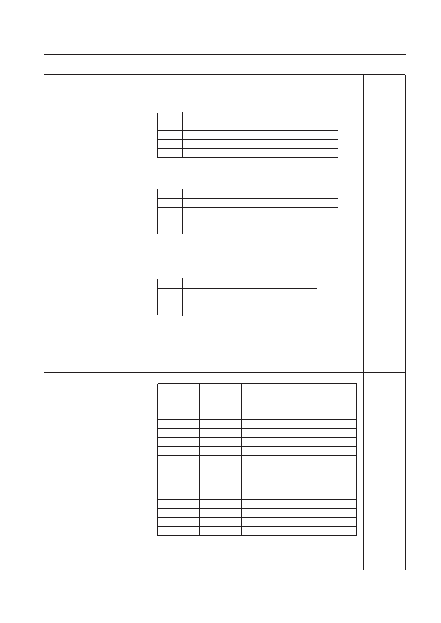
DI control data description
No.
Control block/data
Content
Related data
This data sets the divisor for the programmable divider and P15 is the MSB of this binary
value. LSB will change according to the DVS and SNS.
*: When the LSB is P4, P0 to P3 are invalid.
Used to select programmable divider signal input pins (FMIN, AMIN) and to switch the
input frequency range.
*: When the DVS and SNS are set to 1, the high-speed locking mode is selected, the high-
speed control data becomes valid.
By setting DVS to 1 and SNS to 0 this pin enters FMIN mode, the sub-charge pump
control data is valid, the high-speed locking control data becomes invalid.
(1)
Programmable divider data
P0 to P15
DVS, SNS
This data controls the sub-charge pump.
(* : don’t care)
The sub-charge pump can be used in conjunction with the PDM1 or the PDM2 pin (main
charge pump pin) to form a high-speed locking circuit.
*: FMIN(High-speed mode): Setting DVS and SNS to 1 forces the sub-charge pump to
operate for the time set due to the high-speed locking end flag output wait time, and
allows the locking time to be reduced after switching to the normal PLL mode.
See the “Charge Pump Structure” item for details.
HSE0
HSE1
(2)
Sub-charge pump control data
PDC0, PDC1
Reference frequency selection data
Note: PLL inhibit (backup mode)
The programmable divider block is stopped, the FMIN and AMIN pins are pulled down
to ground, and the charge pump output is set to the floating state.
(3)
Reference divider data
R0 to R3
PDC1
PDC0
Sub-charge pump state
0
*
High impedance
1
Charge pump operating (at all times)
1
0
Charge pump operating (when PLL unlocked)
DVS
SNS
LSB
Set divisor (N)
1
P0
272 to 65535
1
0
P0
272 to 65535
0
1
P0
272 to 65535
0
P4
4 to 4095
DVS
SNS
Input pin
Input pin frequency range
1
FMIN
10 to 160 MHz (High-speed mode)
1
0
FMIN
10 to 160 MHz (Normal mode)
0
1
AMIN
2 to 40 MHz
0
AMIN
0.5 to 10 MHz
R3
R2
R1
R0
Reference frequency (kHz)
0
50
0
1
50
0
1
0
25
0
1
25
0
1
0
12.5
0
1
0
1
6.25
0
1
0
3.125
0
1
3.125
1
0
10
1
0
1
9
1
0
1
0
5
1
0
1
0
3
1
0
1
30
1
0
PLL inhibit + X’tal OSC stop
1
PLL inhibit
Continued on next page.
相关PDF资料 |
PDF描述 |
|---|---|
| LC7216M | PLL FREQUENCY SYNTHESIZER, 40 MHz, PDSO20 |
| LCP-10G3A4EDR | FIBER OPTIC TRANSCEIVER, 840-860nm, 10312.5Mbps(Tx), 10312.5Mbps(Rx), SURFACE MOUNT, LC CONNECTOR |
| LCP-10G3A4EDRH | FIBER OPTIC TRANSCEIVER, 840-860nm, 10312.5Mbps(Tx), 10312.5Mbps(Rx), SURFACE MOUNT, LC CONNECTOR |
| LCP-10G3B4QDR | FIBER OPTIC TRANSCEIVER, 1260-1355nm, 10000Mbps(Tx), 10000Mbps(Rx), SURFACE MOUNT, LC CONNECTOR |
| LCP-10G3B4QDRT | FIBER OPTIC TRANSCEIVER, 1260-1355nm, 10000Mbps(Tx), 10000Mbps(Rx), SURFACE MOUNT, LC CONNECTOR |
相关代理商/技术参数 |
参数描述 |
|---|---|
| LC72151VS-MPB-E | 制造商:ON Semiconductor 功能描述:PLL FREQUENCY SYNTHESIZER - Ammo Pack |
| LC72151VS-TRM-E | 功能描述:时钟合成器/抖动清除器 RoHS:否 制造商:Skyworks Solutions, Inc. 输出端数量: 输出电平: 最大输出频率: 输入电平: 最大输入频率:6.1 GHz 电源电压-最大:3.3 V 电源电压-最小:2.7 V 封装 / 箱体:TSSOP-28 封装:Reel |
| LC7215F | 制造商:SANYO 制造商全称:Sanyo Semicon Device 功能描述:MW/LW PLL Frequency Synthesizers |
| LC7215FM | 制造商:SANYO 制造商全称:Sanyo Semicon Device 功能描述:MW/LW PLL Frequency Synthesizers |
| LC7216M | 制造商:SANYO 制造商全称:Sanyo Semicon Device 功能描述:PLL Frequency Synthesizer for Electronic Tuning |
发布紧急采购,3分钟左右您将得到回复。