- 您现在的位置:买卖IC网 > PDF目录19799 > LCMXO2280C-3BN256I (Lattice Semiconductor Corporation)IC PLD 2280LUTS 211I/O 256CABGA PDF资料下载
参数资料
| 型号: | LCMXO2280C-3BN256I |
| 厂商: | Lattice Semiconductor Corporation |
| 文件页数: | 16/88页 |
| 文件大小: | 0K |
| 描述: | IC PLD 2280LUTS 211I/O 256CABGA |
| 标准包装: | 119 |
| 系列: | MachXO |
| 可编程类型: | 系统内可编程 |
| 最大延迟时间 tpd(1): | 5.1ns |
| 电压电源 - 内部: | 1.71 V ~ 3.465 V |
| 宏单元数: | 1140 |
| 输入/输出数: | 211 |
| 工作温度: | -40°C ~ 100°C |
| 安装类型: | 表面贴装 |
| 封装/外壳: | 256-LFBGA,CSPBGA |
| 供应商设备封装: | 256-CABGA(14x14) |
| 包装: | 托盘 |
| 其它名称: | 220-1073 |
第1页第2页第3页第4页第5页第6页第7页第8页第9页第10页第11页第12页第13页第14页第15页当前第16页第17页第18页第19页第20页第21页第22页第23页第24页第25页第26页第27页第28页第29页第30页第31页第32页第33页第34页第35页第36页第37页第38页第39页第40页第41页第42页第43页第44页第45页第46页第47页第48页第49页第50页第51页第52页第53页第54页第55页第56页第57页第58页第59页第60页第61页第62页第63页第64页第65页第66页第67页第68页第69页第70页第71页第72页第73页第74页第75页第76页第77页第78页第79页第80页第81页第82页第83页第84页第85页第86页第87页第88页
�� �
�
�Architecture�
�MachXO� Family� Data� Sheet�
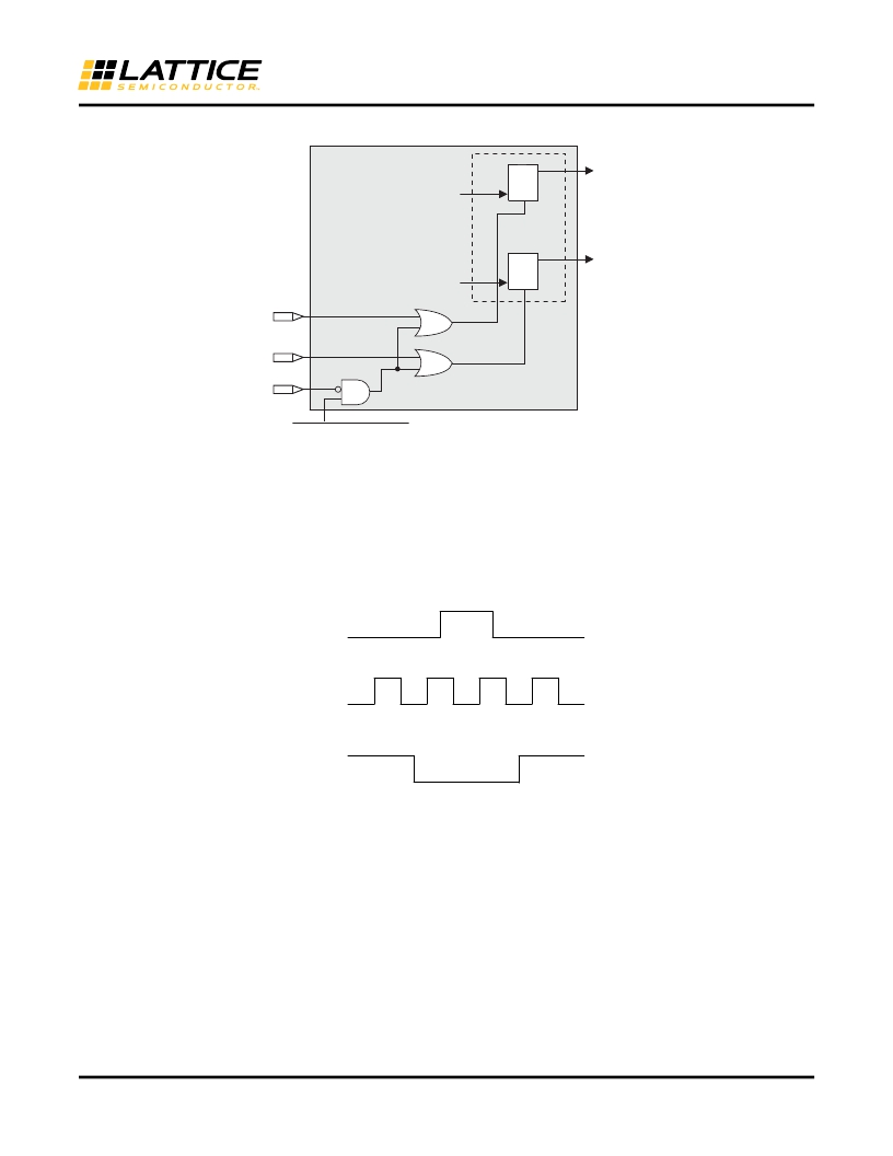
�Figure� 2-13.� Memory� Core� Reset�
�Memory� Core�
�D�
�SET�
�Q�
�Port� A[17:0]�
�L� CLR�
�Output� Data�
�Latches�
�D�
�SET�
�Q�
�Port� B[17:0]�
�L� CLR�
�RSTA�
�RSTB�
�GSRN�
�Programmable� Disable�
�For� further� information� on� the� sysMEM� EBR� block,� see� the� details� of� additional� technical� documentation� at� the� end�
�of� this� data� sheet.�
�EBR� Asynchronous� Reset�
�EBR� asynchronous� reset� or� GSR� (if� used)� can� only� be� applied� if� all� clock� enables� are� low� for� a� clock� cycle� before� the�
�reset� is� applied� and� released� a� clock� cycle� after� the� reset� is� released,� as� shown� in� Figure� 2-14.� The� GSR� input� to� the�
�EBR� is� always� asynchronous.�
�Figure� 2-14.� EBR� Asynchronous� Reset� (Including� GSR)� Timing� Diagram�
�Reset�
�Clock�
�Clock�
�Enable�
�If� all� clock� enables� remain� enabled,� the� EBR� asynchronous� reset� or� GSR� may� only� be� applied� and� released� after�
�the� EBR� read� and� write� clock� inputs� are� in� a� steady� state� condition� for� a� minimum� of� 1/f� MAX� (EBR� clock).� The� reset�
�release� must� adhere� to� the� EBR� synchronous� reset� setup� time� before� the� next� active� read� or� write� clock� edge.�
�If� an� EBR� is� pre-loaded� during� configuration,� the� GSR� input� must� be� disabled� or� the� release� of� the� GSR� during�
�device� Wake� Up� must� occur� before� the� release� of� the� device� I/Os� becoming� active.�
�These� instructions� apply� to� all� EBR� RAM,� ROM� and� FIFO� implementations.� For� the� EBR� FIFO� mode,� the� GSR� sig-�
�nal� is� always� enabled� and� the� WE� and� RE� signals� act� like� the� clock� enable� signals� in� Figure� 2-14.� The� reset� timing�
�rules� apply� to� the� RPReset� input� vs� the� RE� input� and� the� RST� input� vs.� the� WE� and� RE� inputs.� Both� RST� and�
�RPReset� are� always� asynchronous� EBR� inputs.�
�Note� that� there� are� no� reset� restrictions� if� the� EBR� synchronous� reset� is� used� and� the� EBR� GSR� input� is� disabled�
�2-13�
�相关PDF资料 |
PDF描述 |
|---|---|
| LCMXO1200E-4TN100C | IC FPGA 1.2KLUTS 100TQFP |
| GSM36DTAN-S273 | CONN EDGECARD 72POS R/A .156 SLD |
| HMC31DRES-S93 | CONN EDGECARD 62POS .100 EYELET |
| LCMXO1200C-4TN100C | IC PLD 1200LUTS 73I/O 100-TQFP |
| GEC25DRYN-S13 | CONN EDGECARD 50POS .100 EXTEND |
相关代理商/技术参数 |
参数描述 |
|---|---|
| LCMXO2280C-3FT256C | 功能描述:CPLD - 复杂可编程逻辑器件 2280 LUTs 211 IO 1.8 /2.5/3.3V -3 Spd RoHS:否 制造商:Lattice 系列: 存储类型:EEPROM 大电池数量:128 最大工作频率:333 MHz 延迟时间:2.7 ns 可编程输入/输出端数量:64 工作电源电压:3.3 V 最大工作温度:+ 90 C 最小工作温度:0 C 封装 / 箱体:TQFP-100 |
| LCMXO2280C-3FT256I | 功能描述:CPLD - 复杂可编程逻辑器件 2280 LUTs 211 IO 1.8 /2.5/3.3V -3 Spd I RoHS:否 制造商:Lattice 系列: 存储类型:EEPROM 大电池数量:128 最大工作频率:333 MHz 延迟时间:2.7 ns 可编程输入/输出端数量:64 工作电源电压:3.3 V 最大工作温度:+ 90 C 最小工作温度:0 C 封装 / 箱体:TQFP-100 |
| LCMXO2280C-3FT324C | 功能描述:CPLD - 复杂可编程逻辑器件 2280 LUTs 271 IO 1.8 /2.5/3.3V -3 Spd RoHS:否 制造商:Lattice 系列: 存储类型:EEPROM 大电池数量:128 最大工作频率:333 MHz 延迟时间:2.7 ns 可编程输入/输出端数量:64 工作电源电压:3.3 V 最大工作温度:+ 90 C 最小工作温度:0 C 封装 / 箱体:TQFP-100 |
| LCMXO2280C-3FT324I | 功能描述:CPLD - 复杂可编程逻辑器件 2280 LUTs 271 IO 1.8 /2.5/3.3V -3 Spd I RoHS:否 制造商:Lattice 系列: 存储类型:EEPROM 大电池数量:128 最大工作频率:333 MHz 延迟时间:2.7 ns 可编程输入/输出端数量:64 工作电源电压:3.3 V 最大工作温度:+ 90 C 最小工作温度:0 C 封装 / 箱体:TQFP-100 |
| LCMXO2280C-3FTN256C | 功能描述:CPLD - 复杂可编程逻辑器件 2280 LUTS 211 I/O RoHS:否 制造商:Lattice 系列: 存储类型:EEPROM 大电池数量:128 最大工作频率:333 MHz 延迟时间:2.7 ns 可编程输入/输出端数量:64 工作电源电压:3.3 V 最大工作温度:+ 90 C 最小工作温度:0 C 封装 / 箱体:TQFP-100 |
发布紧急采购,3分钟左右您将得到回复。