- 您现在的位置:买卖IC网 > PDF目录177783 > LCMXO2280C-3FT324I (LATTICE SEMICONDUCTOR CORP) PDF资料下载
参数资料
| 型号: | LCMXO2280C-3FT324I |
| 厂商: | LATTICE SEMICONDUCTOR CORP |
| 元件分类: | PLD |
| 中文描述: | FLASH PLD, 5.1 ns, PBGA324 |
| 封装: | 19 X 19 MM, FTBGA-324 |
| 文件页数: | 10/96页 |
| 文件大小: | 1389K |
| 代理商: | LCMXO2280C-3FT324I |
第1页第2页第3页第4页第5页第6页第7页第8页第9页当前第10页第11页第12页第13页第14页第15页第16页第17页第18页第19页第20页第21页第22页第23页第24页第25页第26页第27页第28页第29页第30页第31页第32页第33页第34页第35页第36页第37页第38页第39页第40页第41页第42页第43页第44页第45页第46页第47页第48页第49页第50页第51页第52页第53页第54页第55页第56页第57页第58页第59页第60页第61页第62页第63页第64页第65页第66页第67页第68页第69页第70页第71页第72页第73页第74页第75页第76页第77页第78页第79页第80页第81页第82页第83页第84页第85页第86页第87页第88页第89页第90页第91页第92页第93页第94页第95页第96页
2-15
Architecture
Lattice Semiconductor
MachXO Family Data Sheet
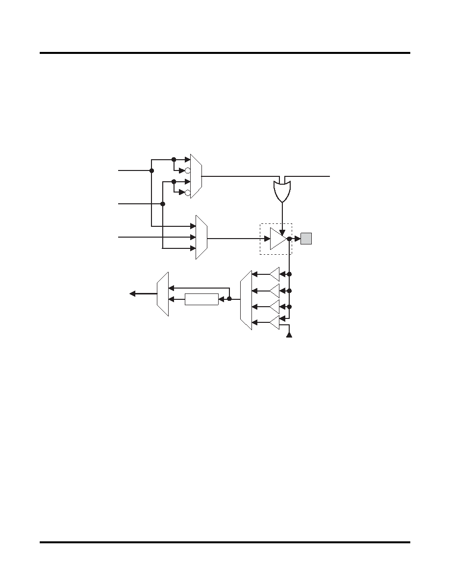
output data signals are multiplexed and provide a single signal to the I/O pin via the sysIO buffer. Figure 2-17
shows the MachXO PIO logic.
The tristate control signal is multiplexed from the output data signals and their complements. In addition a global
signal (TSALL) from a dedicated pad can be used to tristate the sysIO buffer.
The PIO receives an input signal from the pin via the sysIO buffer and provides this signal to the core of the device.
In addition there are programmable elements that can be utilized by the design tools to avoid positive hold times.
Figure 2-17. MachXO PIO Block Diagram
sysIO Buffer
Each I/O is associated with a flexible buffer referred to as a sysIO buffer. These buffers are arranged around the
periphery of the device in groups referred to as Banks. The sysIO buffers allow users to implement the wide variety
of standards that are found in today’s systems including LVCMOS, TTL, BLVDS, LVDS and LVPECL.
In the MachXO devices, single-ended output buffers and ratioed input buffers (LVTTL, LVCMOS and PCI) are pow-
ered using VCCIO. In addition to the Bank VCCIO supplies, the MachXO devices have a VCC core logic power supply,
and a VCCAUX supply that powers up a variety of internal circuits including all the differential and referenced input buf-
fers.
MachXO256 and MachXO640 devices contain single-ended input buffers and single-ended output buffers with
complementary outputs on all the I/O Banks.
MachXO1200 and MachXO2280 devices contain two types of sysIO buffer pairs.
1.
Top and Bottom sysIO Buffer Pairs
The sysIO buffer pairs in the top and bottom Banks of the device consist of two single-ended output drivers and
two sets of single-ended input buffers (for ratioed or absolute input levels). The I/O pairs on the top and bottom
PAD
sysIO
Buffer
TO
Programmable
Delay Elements
From Complementary
Pad
1
2
3
4
+
-
Input
Data Signal
From Routing
Fast Output
Note: Buffer 1 tracks with VCCAUX
Buffer 3 tracks with internal 1.2V VREF.
Buffer 4 is available in MachXO1200 and MachXO2280 devices only.
Buffer 2 tracks with VCCIO.
Data signal
TSALL
DO
TS
相关PDF资料 |
PDF描述 |
|---|---|
| LCMXO640E-4FT256C | |
| LCMXO1200C-4B256I | |
| LCMXO1200E-4M132C | |
| LCMXO1200E-4FT256C | |
| LCMXO1200E-3T144I | |
相关代理商/技术参数 |
参数描述 |
|---|---|
| LCMXO2280C-3FTN256C | 功能描述:CPLD - 复杂可编程逻辑器件 2280 LUTS 211 I/O RoHS:否 制造商:Lattice 系列: 存储类型:EEPROM 大电池数量:128 最大工作频率:333 MHz 延迟时间:2.7 ns 可编程输入/输出端数量:64 工作电源电压:3.3 V 最大工作温度:+ 90 C 最小工作温度:0 C 封装 / 箱体:TQFP-100 |
| LCMXO2280C-3FTN256I | 功能描述:CPLD - 复杂可编程逻辑器件 2280 LUTs 211 IO 1.8 /2.5/3.3V -3 Spd I RoHS:否 制造商:Lattice 系列: 存储类型:EEPROM 大电池数量:128 最大工作频率:333 MHz 延迟时间:2.7 ns 可编程输入/输出端数量:64 工作电源电压:3.3 V 最大工作温度:+ 90 C 最小工作温度:0 C 封装 / 箱体:TQFP-100 |
| LCMXO2280C-3FTN324C | 功能描述:CPLD - 复杂可编程逻辑器件 2280 LUTS 271 I/O RoHS:否 制造商:Lattice 系列: 存储类型:EEPROM 大电池数量:128 最大工作频率:333 MHz 延迟时间:2.7 ns 可编程输入/输出端数量:64 工作电源电压:3.3 V 最大工作温度:+ 90 C 最小工作温度:0 C 封装 / 箱体:TQFP-100 |
| LCMXO2280C-3FTN324I | 功能描述:CPLD - 复杂可编程逻辑器件 2280 LUTs 271 IO 1.8 /2.5/3.3V -3 Spd I RoHS:否 制造商:Lattice 系列: 存储类型:EEPROM 大电池数量:128 最大工作频率:333 MHz 延迟时间:2.7 ns 可编程输入/输出端数量:64 工作电源电压:3.3 V 最大工作温度:+ 90 C 最小工作温度:0 C 封装 / 箱体:TQFP-100 |
| LCMXO2280C-3M132C | 功能描述:CPLD - 复杂可编程逻辑器件 2280 LUTs 101 I/O 1.8/2.5/3.3V -3 Spd RoHS:否 制造商:Lattice 系列: 存储类型:EEPROM 大电池数量:128 最大工作频率:333 MHz 延迟时间:2.7 ns 可编程输入/输出端数量:64 工作电源电压:3.3 V 最大工作温度:+ 90 C 最小工作温度:0 C 封装 / 箱体:TQFP-100 |
发布紧急采购,3分钟左右您将得到回复。