- 您现在的位置:买卖IC网 > PDF目录4569 > LFECP20E-5FN672C (Lattice Semiconductor Corporation)IC FPGA 19.7KLUTS 672FPBGA PDF资料下载
参数资料
| 型号: | LFECP20E-5FN672C |
| 厂商: | Lattice Semiconductor Corporation |
| 文件页数: | 86/163页 |
| 文件大小: | 0K |
| 描述: | IC FPGA 19.7KLUTS 672FPBGA |
| 标准包装: | 40 |
| 系列: | ECP |
| 逻辑元件/单元数: | 19700 |
| RAM 位总计: | 434176 |
| 输入/输出数: | 400 |
| 电源电压: | 1.14 V ~ 1.26 V |
| 安装类型: | 表面贴装 |
| 工作温度: | 0°C ~ 85°C |
| 封装/外壳: | 672-BBGA |
| 供应商设备封装: | 672-FPBGA(27x27) |
第1页第2页第3页第4页第5页第6页第7页第8页第9页第10页第11页第12页第13页第14页第15页第16页第17页第18页第19页第20页第21页第22页第23页第24页第25页第26页第27页第28页第29页第30页第31页第32页第33页第34页第35页第36页第37页第38页第39页第40页第41页第42页第43页第44页第45页第46页第47页第48页第49页第50页第51页第52页第53页第54页第55页第56页第57页第58页第59页第60页第61页第62页第63页第64页第65页第66页第67页第68页第69页第70页第71页第72页第73页第74页第75页第76页第77页第78页第79页第80页第81页第82页第83页第84页第85页当前第86页第87页第88页第89页第90页第91页第92页第93页第94页第95页第96页第97页第98页第99页第100页第101页第102页第103页第104页第105页第106页第107页第108页第109页第110页第111页第112页第113页第114页第115页第116页第117页第118页第119页第120页第121页第122页第123页第124页第125页第126页第127页第128页第129页第130页第131页第132页第133页第134页第135页第136页第137页第138页第139页第140页第141页第142页第143页第144页第145页第146页第147页第148页第149页第150页第151页第152页第153页第154页第155页第156页第157页第158页第159页第160页第161页第162页第163页
2-26
Architecture
LatticeECP/EC Family Data Sheet
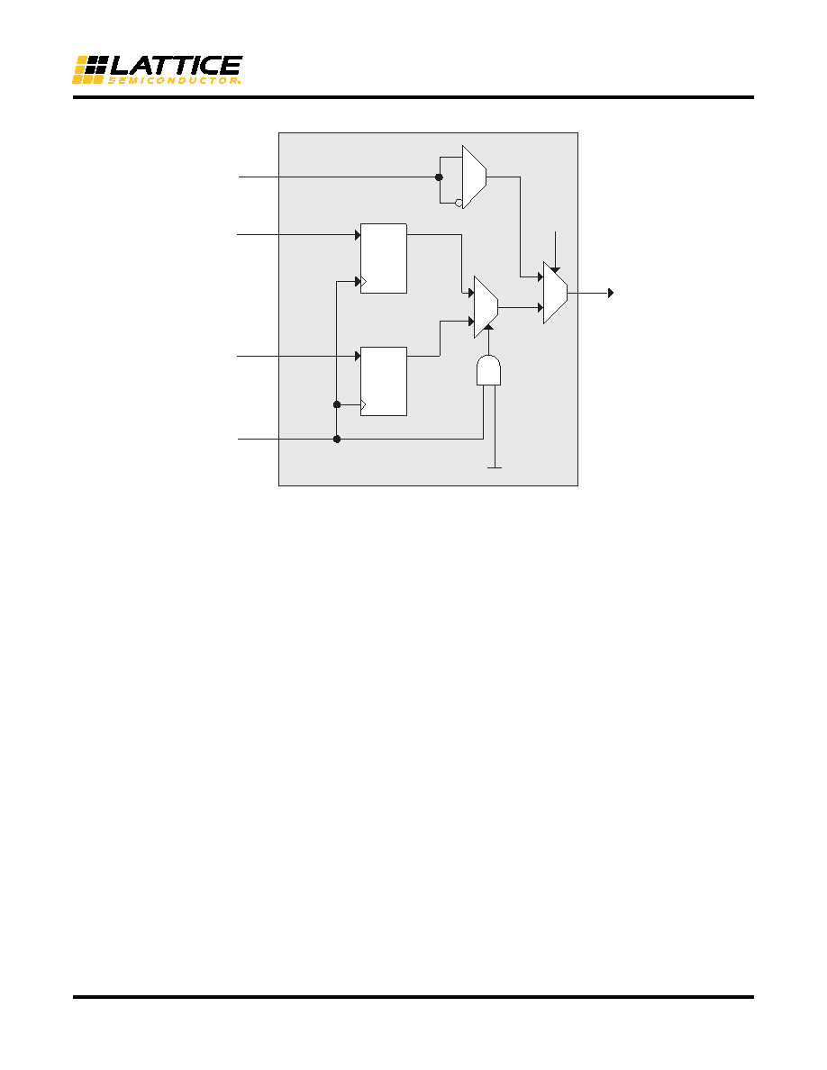
Figure 2-31. Tristate Register Block
Control Logic Block
The control logic block allows the selection and modification of control signals for use in the PIO block. A clock is
selected from one of the clock signals provided from the general purpose routing and a DQS signal provided from
the programmable DQS pin. The clock can optionally be inverted.
The clock enable and local reset signals are selected from the routing and optionally inverted. The global tristate
signal is passed through this block.
DDR Memory Support
Implementing high performance DDR memory interfaces requires dedicated DDR register structures in the input
(for read operations) and in the output (for write operations). As indicated in the PIO Logic section, the LatticeEC
devices provide this capability. In addition to these registers, the LatticeEC devices contain two elements to simplify
the design of input structures for read operations: the DQS delay block and polarity control logic.
DLL Calibrated DQS Delay Block
Source Synchronous interfaces generally require the input clock to be adjusted in order to correctly capture data at
the input register. For most interfaces a PLL is used for this adjustment. However in DDR memories the clock
(referred to as DQS) is not free running so this approach cannot be used. The DQS Delay block provides the
required clock alignment for DDR memory interfaces.
The DQS signal (selected PIOs only) feeds from the PAD through a DQS delay element to a dedicated DQS routing
resource. The DQS signal also feeds polarity control logic, which controls the polarity of the clock to the sync regis-
ters in the input register blocks. Figures 2-32 and 2-33 show how the DQS transition signals are routed to the PIOs.
The temperature, voltage and process variations of the DQS delay block are compensated by a set of calibration
(6-bit bus) signals from two DLLs on opposite sides of the device. Each DLL compensates DQS Delays in its half of
the device as shown in Figure 2-33. The DLL loop is compensated for temperature, voltage and process variations
by the system clock and feedback loop.
D
LE*
Q
D
Q
D-Type
ONEG1
CLK1
Programmed
Control
TO
Latch
*Latch is transparent when input is low.
OPOS1
OUTDDN
/LATCH
0
1
0
1
From
Routing
To sysIO
Buffer
TD
相关PDF资料 |
PDF描述 |
|---|---|
| RSC49DRTN-S734 | CONN EDGECARD 98POS DIP .100 SLD |
| RMC49DRTN-S734 | CONN EDGECARD 98POS DIP .100 SLD |
| RSC49DRTH-S734 | CONN EDGECARD 98POS DIP .100 SLD |
| RMC49DRTH-S734 | CONN EDGECARD 98POS DIP .100 SLD |
| MAX9952DCCB+T | IC PMU DUAL 64TQFP |
相关代理商/技术参数 |
参数描述 |
|---|---|
| LFECP20E-5FN672I | 制造商:LATTICE 制造商全称:Lattice Semiconductor 功能描述:LatticeECP/EC Family Data Sheet |
| LFECP20E-5Q208C | 制造商:LATTICE 制造商全称:Lattice Semiconductor 功能描述:LatticeECP/EC Family Data Sheet |
| LFECP20E-5Q208I | 制造商:LATTICE 制造商全称:Lattice Semiconductor 功能描述:LatticeECP/EC Family Data Sheet |
| LFECP20E-5QN208C | 制造商:LATTICE 制造商全称:Lattice Semiconductor 功能描述:LatticeECP/EC Family Data Sheet |
| LFECP20E-5QN208I | 制造商:LATTICE 制造商全称:Lattice Semiconductor 功能描述:LatticeECP/EC Family Data Sheet |
发布紧急采购,3分钟左右您将得到回复。