- 您现在的位置:买卖IC网 > PDF目录4569 > LFECP20E-5FN672C (Lattice Semiconductor Corporation)IC FPGA 19.7KLUTS 672FPBGA PDF资料下载
参数资料
| 型号: | LFECP20E-5FN672C |
| 厂商: | Lattice Semiconductor Corporation |
| 文件页数: | 90/163页 |
| 文件大小: | 0K |
| 描述: | IC FPGA 19.7KLUTS 672FPBGA |
| 标准包装: | 40 |
| 系列: | ECP |
| 逻辑元件/单元数: | 19700 |
| RAM 位总计: | 434176 |
| 输入/输出数: | 400 |
| 电源电压: | 1.14 V ~ 1.26 V |
| 安装类型: | 表面贴装 |
| 工作温度: | 0°C ~ 85°C |
| 封装/外壳: | 672-BBGA |
| 供应商设备封装: | 672-FPBGA(27x27) |
第1页第2页第3页第4页第5页第6页第7页第8页第9页第10页第11页第12页第13页第14页第15页第16页第17页第18页第19页第20页第21页第22页第23页第24页第25页第26页第27页第28页第29页第30页第31页第32页第33页第34页第35页第36页第37页第38页第39页第40页第41页第42页第43页第44页第45页第46页第47页第48页第49页第50页第51页第52页第53页第54页第55页第56页第57页第58页第59页第60页第61页第62页第63页第64页第65页第66页第67页第68页第69页第70页第71页第72页第73页第74页第75页第76页第77页第78页第79页第80页第81页第82页第83页第84页第85页第86页第87页第88页第89页当前第90页第91页第92页第93页第94页第95页第96页第97页第98页第99页第100页第101页第102页第103页第104页第105页第106页第107页第108页第109页第110页第111页第112页第113页第114页第115页第116页第117页第118页第119页第120页第121页第122页第123页第124页第125页第126页第127页第128页第129页第130页第131页第132页第133页第134页第135页第136页第137页第138页第139页第140页第141页第142页第143页第144页第145页第146页第147页第148页第149页第150页第151页第152页第153页第154页第155页第156页第157页第158页第159页第160页第161页第162页第163页
2-29
Architecture
LatticeECP/EC Family Data Sheet
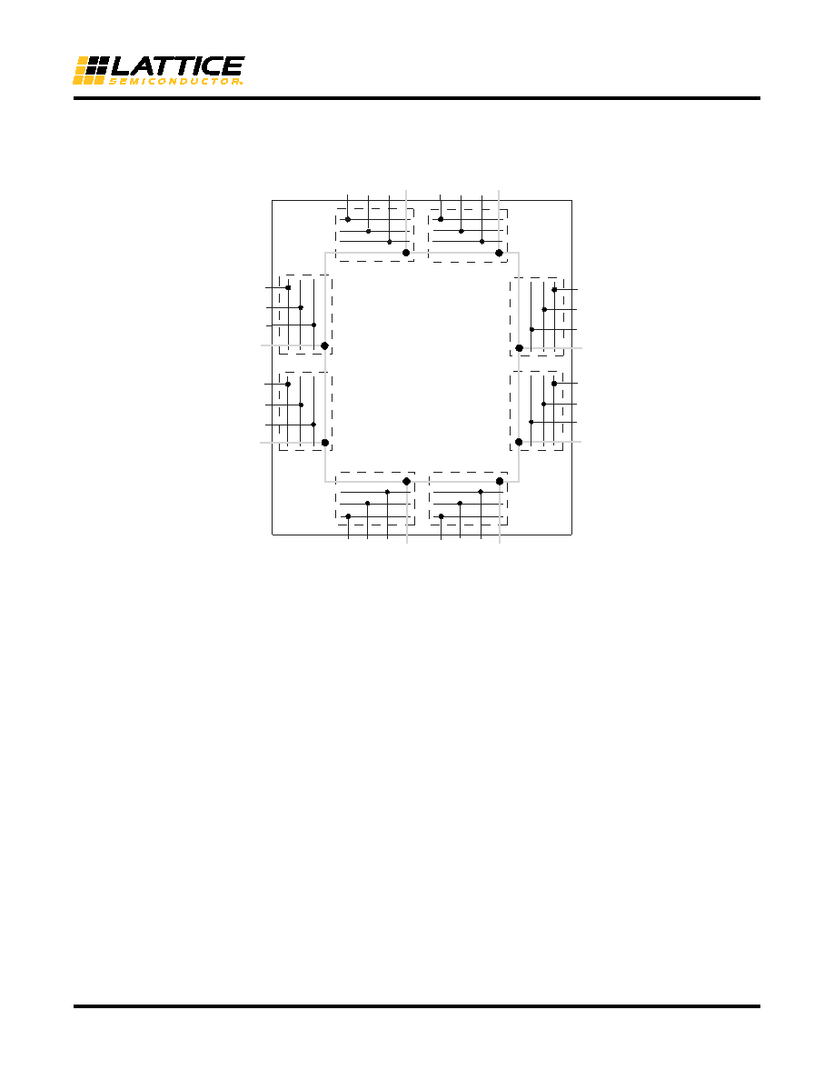
Figure 2-34. LatticeECP/EC Banks
LatticeECP/EC devices contain two types of sysI/O buffer pairs.
1.
Top and Bottom sysI/O Buffer Pairs (Single-Ended Outputs Only)
The sysI/O buffer pairs in the top and bottom banks of the device consist of two single-ended output drivers
and two sets of single-ended input buffers (both ratioed and referenced). The referenced input buffer can also
be configured as a differential input.
The two pads in the pair are described as “true” and “comp”, where the true pad is associated with the positive
side of the differential input buffer and the comp (complementary) pad is associated with the negative side of
the differential input buffer.
Only the I/Os on the top and bottom banks have programmable PCI clamps. These I/O banks also support hot
socketing with IDK less than 1mA. Note that the PCI clamp is enabled after VCC, VCCAUX and VCCIO are at valid
operating levels and the device has been configured.
2.
Left and Right sysI/O Buffer Pairs (Differential and Single-Ended Outputs)
The sysI/O buffer pairs in the left and right banks of the device consist of two single-ended output drivers, two
sets of single-ended input buffers (both ratioed and referenced) and one differential output driver. The refer-
enced input buffer can also be configured as a differential input. In these banks the two pads in the pair are
described as “true” and “comp”, where the true pad is associated with the positive side of the differential I/O,
and the comp (complementary) pad is associated with the negative side of the differential I/O.
Only the left and right banks have LVDS differential output drivers. See the IDK specification for I/O leakage cur-
rent during power-up.
V
REF1(2)
GND
Bank
2
V
CCIO2
V
REF2(2)
V
REF1(3)
GND
Bank
3
V
CCIO3
V
REF2(3)
V
REF1(7)
GND
TOP
LEFT
RIGHT
BOTTOM
Bank
7
V
CCIO7
V
REF2(7)
V
REF1(6)
GND
Bank
6
V
CCIO6
V
REF2(6)
V
REF1(5)
GND
Bank 5
V
CCIO5
V
REF2(5)
V
REF1(4)
GND
Bank 4
V
CCIO4
V
REF2(4)
V
REF1(0)
GND
Bank 0
V
CCIO0
V
REF2(0)
V
REF1(1)
GND
Bank 1
V
CCIO1
V
REF2(1)
相关PDF资料 |
PDF描述 |
|---|---|
| RSC49DRTN-S734 | CONN EDGECARD 98POS DIP .100 SLD |
| RMC49DRTN-S734 | CONN EDGECARD 98POS DIP .100 SLD |
| RSC49DRTH-S734 | CONN EDGECARD 98POS DIP .100 SLD |
| RMC49DRTH-S734 | CONN EDGECARD 98POS DIP .100 SLD |
| MAX9952DCCB+T | IC PMU DUAL 64TQFP |
相关代理商/技术参数 |
参数描述 |
|---|---|
| LFECP20E-5FN672I | 制造商:LATTICE 制造商全称:Lattice Semiconductor 功能描述:LatticeECP/EC Family Data Sheet |
| LFECP20E-5Q208C | 制造商:LATTICE 制造商全称:Lattice Semiconductor 功能描述:LatticeECP/EC Family Data Sheet |
| LFECP20E-5Q208I | 制造商:LATTICE 制造商全称:Lattice Semiconductor 功能描述:LatticeECP/EC Family Data Sheet |
| LFECP20E-5QN208C | 制造商:LATTICE 制造商全称:Lattice Semiconductor 功能描述:LatticeECP/EC Family Data Sheet |
| LFECP20E-5QN208I | 制造商:LATTICE 制造商全称:Lattice Semiconductor 功能描述:LatticeECP/EC Family Data Sheet |
发布紧急采购,3分钟左右您将得到回复。