- 您现在的位置:买卖IC网 > PDF目录67755 > LM12438CIWMX (NATIONAL SEMICONDUCTOR CORP) SPECIALTY ANALOG CIRCUIT, PDSO28 PDF资料下载
参数资料
| 型号: | LM12438CIWMX |
| 厂商: | NATIONAL SEMICONDUCTOR CORP |
| 元件分类: | 模拟信号调理 |
| 英文描述: | SPECIALTY ANALOG CIRCUIT, PDSO28 |
| 封装: | SOP-28 |
| 文件页数: | 17/80页 |
| 文件大小: | 1552K |
| 代理商: | LM12438CIWMX |
第1页第2页第3页第4页第5页第6页第7页第8页第9页第10页第11页第12页第13页第14页第15页第16页当前第17页第18页第19页第20页第21页第22页第23页第24页第25页第26页第27页第28页第29页第30页第31页第32页第33页第34页第35页第36页第37页第38页第39页第40页第41页第42页第43页第44页第45页第46页第47页第48页第49页第50页第51页第52页第53页第54页第55页第56页第57页第58页第59页第60页第61页第62页第63页第64页第65页第66页第67页第68页第69页第70页第71页第72页第73页第74页第75页第76页第77页第78页第79页第80页
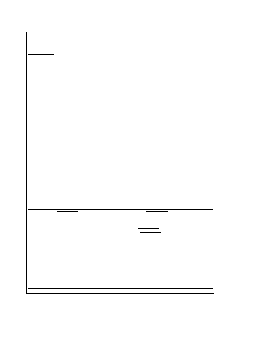
50 Pin Descriptions (Continued)
TABLE I LM12 L 438 Pin Description
(Continued)
Pin Number
Pin Name
Description
PLCC
SO
Pkg
20
26
P2
Serial interface input
Standard
CS
8051
1
I2C
SAD1
TMS320
FSX
21
27
P1
Serial interface input
Standard
R F (Clock risefall)
8051
1
I2C
SAD0
TMS320
FSR
22
28
MODESEL2
Serial mode selection inputs The logic states of these inputs determine the operation of
23
1
MODESEL1
the serial mode as shown below The standard mode covers the National’s MICROWIRE
Motorola’s SPI and Hitachi’s SCl protocols
MODESEL1 MODESEL2
01
Standard mode
00
8051
10
I2C
11
TMS320
24
2
CLK
The device main clock input The operating range of clock frequency is 005 MHz to
100 MHz The device accuracy is guaranteed only for the clock frequencies indicated in
the specification tables
25
3
INT
Interrupt output This is an active low output An interrupt is generated any time a non-
masked interrupt condition takes place There are seven different conditions that can
generate an interrupt (Refer to Section 624) The interrupt is set high (inactive) by reading
the interrupt status register This output can drive up to 100 pF of capacitive loads An
external buffer should be used for driving higher capacitive loads
26
4
SYNC
Synchronization inputoutput SYNC is an input if the Configuration Register’s SYNC IO bit
is ‘‘0’’ and output when the bit is ‘‘1’’ When sync is an input a rising edge on this pin
causes the internal SH to hold the input signal and a conversion cycle or a comparison
cycle (depending on the programmed instruction) to be started (The conversion or
comparison actually begins on the rising edge of the CLK immediately following the rising
edge of sync) When output it goes high at the start of a conversion or a comparison cycle
and returns low when the cycle is completed At power up the SYNC pin is set as an input
When used as an output it can drive up to 100 pF of capacitive loads An external buffer
should be used for driving higher capacitive loads
27
5
STANDBYOUT
Stand-by output This is an active low output STANDBYOUT will be activated when the
LM12 L 438 is put into stand-by mode through the Configuration Register’s stand-by bit It
is used to force any other devices in the system (signal conditioning circuitry for example)
to go into power-down mode This is done by connecting the ‘‘shutdown’’ ‘‘powerdown’’
‘‘standby’’ etc pins of the other ICs to STANDBYOUT In those cases where the peripheral
ICs do not have the power-down inputs STANDBYOUT can be used to turn off their power
through an electronic switch Note that the logic polarity of the STANDBYOUT is the
opposite to that of the stand-by bit in the Configuration Register
28
6
VDa
Digital supply See above definition
LM12434 Pin Description (Same as LM12 L 438 with the exceptions of the following pins)
LM12434 Pin Description (Same As LM12 L 438 with the exception of the following pins)
6
12
MUXOUTb
Multiplexer outputs These are the LM12434’s externally available analog MUX output pins
7
13
MUXOUTa
Analog inputs are directed to these outputs based on the Instruction RAM programming
8
14
SH INb
Sample-and-hold inputs These are the inverting and non-inverting inputs of the sample-
9
15
SH INa
and-hold LM12434 allows external analog signal conditioning circuits to be placed
between MUX outputs and SH inputs
24
相关PDF资料 |
PDF描述 |
|---|---|
| LM12434CIWMX | SPECIALTY ANALOG CIRCUIT, PDSO28 |
| LM12L438CIWMX | SPECIALTY ANALOG CIRCUIT, PDSO28 |
| LM20323AMHX | 6 A SWITCHING REGULATOR, 570 kHz SWITCHING FREQ-MAX, PDSO20 |
| LM20323AMHE | 6 A SWITCHING REGULATOR, 570 kHz SWITCHING FREQ-MAX, PDSO20 |
| LM20323AMH | 6 A SWITCHING REGULATOR, 570 kHz SWITCHING FREQ-MAX, PDSO20 |
相关代理商/技术参数 |
参数描述 |
|---|---|
| LM12454 | 制造商:未知厂家 制造商全称:未知厂家 功能描述:General Purpose Controller Z84C15 |
| LM12454_06 | 制造商:NSC 制造商全称:National Semiconductor 功能描述:12-Bit + Sign Data Acquisition System with Self-Calibration |
| LM12454A WAF | 制造商:Texas Instruments 功能描述: |
| LM12454CIV | 功能描述:IC ACQUISITION SYS 12BIT 44-PLCC RoHS:否 类别:集成电路 (IC) >> 数据采集 - ADCs/DAC - 专用型 系列:- 产品培训模块:Lead (SnPb) Finish for COTS Obsolescence Mitigation Program 标准包装:50 系列:- 类型:数据采集系统(DAS) 分辨率(位):16 b 采样率(每秒):21.94k 数据接口:MICROWIRE?,QSPI?,串行,SPI? 电压电源:模拟和数字 电源电压:1.8 V ~ 3.6 V 工作温度:-40°C ~ 85°C 安装类型:表面贴装 封装/外壳:40-WFQFN 裸露焊盘 供应商设备封装:40-TQFN-EP(6x6) 包装:托盘 |
| LM12458 | 制造商:NSC 制造商全称:National Semiconductor 功能描述:12-Bit Sign Data Acquisition System with Self-Calibration |
发布紧急采购,3分钟左右您将得到回复。