- 您现在的位置:买卖IC网 > PDF目录67755 > LM12438CIWMX (NATIONAL SEMICONDUCTOR CORP) SPECIALTY ANALOG CIRCUIT, PDSO28 PDF资料下载
参数资料
| 型号: | LM12438CIWMX |
| 厂商: | NATIONAL SEMICONDUCTOR CORP |
| 元件分类: | 模拟信号调理 |
| 英文描述: | SPECIALTY ANALOG CIRCUIT, PDSO28 |
| 封装: | SOP-28 |
| 文件页数: | 37/80页 |
| 文件大小: | 1552K |
| 代理商: | LM12438CIWMX |
第1页第2页第3页第4页第5页第6页第7页第8页第9页第10页第11页第12页第13页第14页第15页第16页第17页第18页第19页第20页第21页第22页第23页第24页第25页第26页第27页第28页第29页第30页第31页第32页第33页第34页第35页第36页当前第37页第38页第39页第40页第41页第42页第43页第44页第45页第46页第47页第48页第49页第50页第51页第52页第53页第54页第55页第56页第57页第58页第59页第60页第61页第62页第63页第64页第65页第66页第67页第68页第69页第70页第71页第72页第73页第74页第75页第76页第77页第78页第79页第80页
70 Digital Interface (Continued)
In both cases the data transfer is insensitive to idle state of
the SCLK SCLK can stay at either logic level high or low
when not clocking (see
Figure 11 )
Data transfer in this mode is basically byte-oriented This is
compatible with the serial interface of the target microcon-
trolIers and microprocessors As mentioned the LM12434
and LM12 L 438 have three different communication cy-
cles write cycle read cycle and burst read cycle At the
start of each data transfer cycle ‘‘command byte’’ is written
to the serial DAS followed by write or read data The com-
mand byte informs the LM12434 and LM12 L 438 about
the communication cycle The command byte carries the
following information
what type of data transfer (communication cycle) is start-
ed
which device register to be accessed
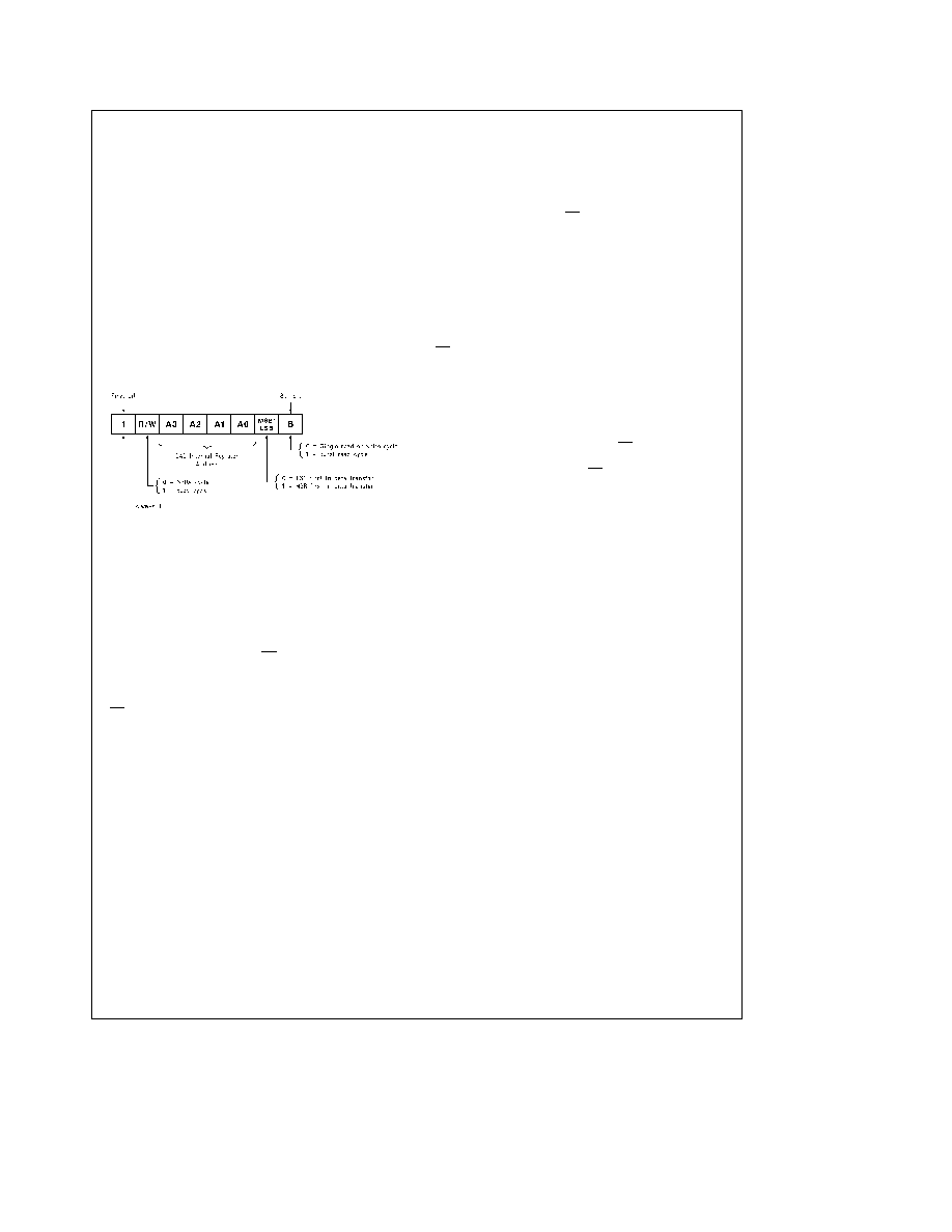
The command byte has the following format
TLH11879 – 52
Note that the first bit may be either the MSB or the LSB of
the byte depending on the processor type but it must be the
first bit transmitted to the LM12434 and LM12 L 438
Figure 11 shows the timing diagrams for different communi-
cation cycles
Figures 11a b c d show write cycles for
various combinations of RF pin logic level and SCLK idle
state
Figures 11e f g h show read cycles for similar sets
of conditions
Figure 11i shows a burst read cycle for the
case of RF e 0 and low SCLK idle state Note that these
timing diagrams depict general relationships between the
SCLK edges the data bits and CS These diagrams are not
meant to show guaranteed timing (See specification tables
for parametric switching characteristics)
Write cycle
A write cycle begins with the falling edge of
CS Then a command byte is written to the DAS on the DI
line synchronized by SCLK The command byte has the
RW and B bits equal to zero Following the command byte
16 bits of data (2 bytes) is shifted in on the same DI line
This data is written to the register addressed in the com-
mand byte (A3 A2 A1 A0) The data is interpreted as MSB
or LSB first based on the logic level of the 7th bit (MSB
LSB) in the command byte There is no activity on the DO
line during write cycles and the DAS leaves the DO line in
the high impedance state CS will go high after the transfer
of the last bit thus completing the write cycle
Read cycle
A read cycle starts the same way as a write
cycle except that the command byte’s RW bits equal to
one Following the command byte the DAS outputs the
data on the DO line synchronized with the microcontroller’s
SCLK The data is read from the register addressed in the
command byte Data is shifted out MSB or LSB first de-
pending on the logic level of the MSBLSB bit The logic
state of the Dl line is ‘‘don’t care’’ after the command byte
CS will go high after the transfer of the last data bit then
completing the read cycle
Burst read cycle
A burst read cycle starts the same way
as a single read cycle but the B bit in the command byte is
set to one indicating a burst read cycle Following the com-
mand byte the data is output on the DO line as long as the
DAS receives SCLK from the system To tell the DAS when
a burst read cycle is completed pull CS high after the 8th
and before the 15th SCLK cycle during the last data byte
transfer (see
Figure 11i ) After CS high is detected and the
last data bit is transferred the DAS is ready for a new com-
munication cycle to begin
The timing diagrams in
Figure 11 show the transfer of data
in packets of 8 bits (bytes) This represents the way the
serial ports of most microcontrollers and microprocessors
produce serial clock and data The DAS does not require a
gap between the first and second byte of the data 16 con-
tinuous clock cycles will transfer the data word However
there should be a gap equal to 3 CLK (the DAS main clock
input not the SCLK) cycles between the end of the com-
mand byte and the start of the data during a read cycle This
is not a concern in most systems for two reasons First the
processor generally has some inherent gap between byte
transfers Second the SCLK frequency is usually signifi-
cantly slower than the CLK frequency For example a
68HC11 processor with an 8 MHz crystal generates a maxi-
mum SCLK frequency of 1 MHz If the DAS is running with a
6 MHz CLK there are 6 cycles of CLK within each cycle of
SCLK and the requirement is satisfied even if SCLK oper-
ates continuously during and after the command byte
42
相关PDF资料 |
PDF描述 |
|---|---|
| LM12434CIWMX | SPECIALTY ANALOG CIRCUIT, PDSO28 |
| LM12L438CIWMX | SPECIALTY ANALOG CIRCUIT, PDSO28 |
| LM20323AMHX | 6 A SWITCHING REGULATOR, 570 kHz SWITCHING FREQ-MAX, PDSO20 |
| LM20323AMHE | 6 A SWITCHING REGULATOR, 570 kHz SWITCHING FREQ-MAX, PDSO20 |
| LM20323AMH | 6 A SWITCHING REGULATOR, 570 kHz SWITCHING FREQ-MAX, PDSO20 |
相关代理商/技术参数 |
参数描述 |
|---|---|
| LM12454 | 制造商:未知厂家 制造商全称:未知厂家 功能描述:General Purpose Controller Z84C15 |
| LM12454_06 | 制造商:NSC 制造商全称:National Semiconductor 功能描述:12-Bit + Sign Data Acquisition System with Self-Calibration |
| LM12454A WAF | 制造商:Texas Instruments 功能描述: |
| LM12454CIV | 功能描述:IC ACQUISITION SYS 12BIT 44-PLCC RoHS:否 类别:集成电路 (IC) >> 数据采集 - ADCs/DAC - 专用型 系列:- 产品培训模块:Lead (SnPb) Finish for COTS Obsolescence Mitigation Program 标准包装:50 系列:- 类型:数据采集系统(DAS) 分辨率(位):16 b 采样率(每秒):21.94k 数据接口:MICROWIRE?,QSPI?,串行,SPI? 电压电源:模拟和数字 电源电压:1.8 V ~ 3.6 V 工作温度:-40°C ~ 85°C 安装类型:表面贴装 封装/外壳:40-WFQFN 裸露焊盘 供应商设备封装:40-TQFN-EP(6x6) 包装:托盘 |
| LM12458 | 制造商:NSC 制造商全称:National Semiconductor 功能描述:12-Bit Sign Data Acquisition System with Self-Calibration |
发布紧急采购,3分钟左右您将得到回复。