- 您现在的位置:买卖IC网 > PDF目录67755 > LM12438CIWMX (NATIONAL SEMICONDUCTOR CORP) SPECIALTY ANALOG CIRCUIT, PDSO28 PDF资料下载
参数资料
| 型号: | LM12438CIWMX |
| 厂商: | NATIONAL SEMICONDUCTOR CORP |
| 元件分类: | 模拟信号调理 |
| 英文描述: | SPECIALTY ANALOG CIRCUIT, PDSO28 |
| 封装: | SOP-28 |
| 文件页数: | 28/80页 |
| 文件大小: | 1552K |
| 代理商: | LM12438CIWMX |
第1页第2页第3页第4页第5页第6页第7页第8页第9页第10页第11页第12页第13页第14页第15页第16页第17页第18页第19页第20页第21页第22页第23页第24页第25页第26页第27页当前第28页第29页第30页第31页第32页第33页第34页第35页第36页第37页第38页第39页第40页第41页第42页第43页第44页第45页第46页第47页第48页第49页第50页第51页第52页第53页第54页第55页第56页第57页第58页第59页第60页第61页第62页第63页第64页第65页第66页第67页第68页第69页第70页第71页第72页第73页第74页第75页第76页第77页第78页第79页第80页
60 Operational Information (Continued)
Bits 12 – 15
store the user-programmable acquisition time
The Sequencer keeps the internal SH in the acquisition
mode for a fixed number of clock cycles (nine clock cycles
for 12-bit a sign conversions and two clock cycles for 8-bit
a
sign conversions or ‘‘watchdog’’ comparisons) plus a
variable number of clock cycles equal to twice the value
stored in Bits 12 – 15 Thus the SH’s acquisition time is (9
a
2D) clock cycles for 12-bit a sign conversions and (2 a
2D) clock cycles for 8-bit a sign conversions or ‘‘watch-
dog’’ comparisons where D is the value stored in Bits 12 –
15 The minimum acquisition time compensates for the typi-
cal internal multiplexer series resistance of 2 kX and any
additional delay created by Bits 12 – 15 compensates for
source resistances greater than 60X 80X
The necessary
acquisition time is determined by the source impedance at
the multiplexer input If the source resistance RS k 60X
and the clock frequency is 8 MHz the value stored in bits
12 – 15 (D) can be 0000 If RS l 60X the following equa-
tions determine the value that should be stored in
bits 12 – 15
D e 045 x RS xfCLK
for 12-bits a sign
D e 036 x RS xfCLK
for 8-bits a sign and ‘‘watchdog’’
RS is in kX and fCLK is in MHz Round the result to the next
higher integer value If the value of 0 obtained from the
expressions above is greater than 15 it is advisable to lower
the source impedance by using an analog buffer between
the signal source and the LM12 L 438’s multiplexer inputs
The value of D can also be used to compensate for the
settling or response time of external processing circuits con-
nected between the LM12434’s MUXOUT and SH IN pins
Instruction RAM Bank 2 RP e 01
The second Instruction RAM section is selected by placing
‘‘01’’ in Bits 8 and 9 of the Configuration register
Bits 0 – 7
hold ‘‘watchdog’’ limit
1
When Bit 11 of Instruc-
tion RAM ‘‘00’’ is set to a ‘‘1’’
the LM12434 and
LM12 L 438 performs a ‘‘watchdog’’ comparison of the
sampled analog input signal with the limit
1 value first
followed by a comparison of the same sampled analog input
signal with the value found in limit
2 (Instruction RAM
‘‘10’’)
Bit 8
holds limit
1’s sign
Bit 9
’s state determines the limit condition that generates a
‘‘watchdog’’ interrupt A ‘‘1’’ causes a voltage greater than
limit
1 to generate an interrupt while a ‘‘0’’ causes a volt-
age less than limit
1 to generate an interrupt
Bits 10 – 15
are not used
Instruction RAM Bank 3 RP e 10
The third Instruction RAM section is selected by placing
‘‘10’’ in Bits 8 and 9 of the Configuration register
Bits 0 – 7
hold ‘‘watchdog’’ limit
2
When Bit 11 of Instruc-
tion RAM ‘‘00’’ is set to a ‘‘1’’
the LM12434 and
LM12 L 438 performs a ‘‘watchdog’’ comparison of the
sampled analog input signal with the limit
1 value first (In-
struction RAM ‘‘01’’) followed by a comparison of the same
sampled analog input signal with the value found in limit
2
Bit 8
holds limit
2’s sign
Bit 9
’s state determines the limit condition that generates a
‘‘watchdog’’ interrupt A ‘‘1’’ causes a voltage greater than
limit
2 to generate an interrupt while a ‘‘0’’ causes a volt-
age less than limit
2 to generate an interrupt
Bits 10 – 15
are not used
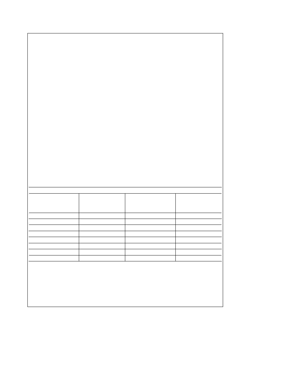
TABLE III LM12 L 438 Operating Mode Input Channel Selection through Input Multiplexer
Normal Operating Mode
Non-Inverting Input
Input Channel to Be
Inverting Input
Input Channel to Be
Channel Selection Bits
Connected to AD
Channel Selection Bits
Connected to AD
in Instruction Register
Non-Inverting Input
in Instruction Register
Inverting Input
D4 D3 D2
(INa)
D7 D6 D5
(INb)
000
IN0
000
GND
001
IN1
001
IN1
010
IN2
010
IN2
011
IN3
011
IN3
100
IN4
100
IN4
101
IN5
101
IN5
110
IN6
110
IN6
111
IN7
111
IN7
34
相关PDF资料 |
PDF描述 |
|---|---|
| LM12434CIWMX | SPECIALTY ANALOG CIRCUIT, PDSO28 |
| LM12L438CIWMX | SPECIALTY ANALOG CIRCUIT, PDSO28 |
| LM20323AMHX | 6 A SWITCHING REGULATOR, 570 kHz SWITCHING FREQ-MAX, PDSO20 |
| LM20323AMHE | 6 A SWITCHING REGULATOR, 570 kHz SWITCHING FREQ-MAX, PDSO20 |
| LM20323AMH | 6 A SWITCHING REGULATOR, 570 kHz SWITCHING FREQ-MAX, PDSO20 |
相关代理商/技术参数 |
参数描述 |
|---|---|
| LM12454 | 制造商:未知厂家 制造商全称:未知厂家 功能描述:General Purpose Controller Z84C15 |
| LM12454_06 | 制造商:NSC 制造商全称:National Semiconductor 功能描述:12-Bit + Sign Data Acquisition System with Self-Calibration |
| LM12454A WAF | 制造商:Texas Instruments 功能描述: |
| LM12454CIV | 功能描述:IC ACQUISITION SYS 12BIT 44-PLCC RoHS:否 类别:集成电路 (IC) >> 数据采集 - ADCs/DAC - 专用型 系列:- 产品培训模块:Lead (SnPb) Finish for COTS Obsolescence Mitigation Program 标准包装:50 系列:- 类型:数据采集系统(DAS) 分辨率(位):16 b 采样率(每秒):21.94k 数据接口:MICROWIRE?,QSPI?,串行,SPI? 电压电源:模拟和数字 电源电压:1.8 V ~ 3.6 V 工作温度:-40°C ~ 85°C 安装类型:表面贴装 封装/外壳:40-WFQFN 裸露焊盘 供应商设备封装:40-TQFN-EP(6x6) 包装:托盘 |
| LM12458 | 制造商:NSC 制造商全称:National Semiconductor 功能描述:12-Bit Sign Data Acquisition System with Self-Calibration |
发布紧急采购,3分钟左右您将得到回复。