- 您现在的位置:买卖IC网 > PDF目录80315 > LM2596-3.3MWC (NATIONAL SEMICONDUCTOR CORP) 7.5 A SWITCHING REGULATOR, 173 kHz SWITCHING FREQ-MAX, UUC PDF资料下载
参数资料
| 型号: | LM2596-3.3MWC |
| 厂商: | NATIONAL SEMICONDUCTOR CORP |
| 元件分类: | 稳压器 |
| 英文描述: | 7.5 A SWITCHING REGULATOR, 173 kHz SWITCHING FREQ-MAX, UUC |
| 封装: | WAFER |
| 文件页数: | 15/36页 |
| 文件大小: | 827K |
| 代理商: | LM2596-3.3MWC |
第1页第2页第3页第4页第5页第6页第7页第8页第9页第10页第11页第12页第13页第14页当前第15页第16页第17页第18页第19页第20页第21页第22页第23页第24页第25页第26页第27页第28页第29页第30页第31页第32页第33页第34页第35页第36页
Application Information (Continued)
DISCONTINUOUS MODE OPERATION
The selection guide chooses inductor values suitable for
continuous mode operation, but for low current applications
and/or high input voltages, a discontinuous mode design
may be a better choice. It would use an inductor that would
be physically smaller, and would need only one half to one
third the inductance value needed for a continuous mode
design. The peak switch and inductor currents will be higher
in a discontinuous design, but at these low load currents (1A
and below), the maximum switch current will still be less than
the switch current limit.
Discontinuous operation can have voltage waveforms that
are considerable different than a continuous design. The
output pin (switch) waveform can have some damped sinu-
soidal ringing present. (See Typical Performance Character-
istics photo titled Discontinuous Mode Switching Wave-
forms) This ringing is normal for discontinuous operation,
and is not caused by feedback loop instabilities. In discon-
tinuous operation, there is a period of time where neither the
switch or the diode are conducting, and the inductor current
has dropped to zero. During this time, a small amount of
energy can circulate between the inductor and the switch/
diode parasitic capacitance causing this characteristic ring-
ing. Normally this ringing is not a problem, unless the ampli-
tude becomes great enough to exceed the input voltage, and
even then, there is very little energy present to cause dam-
age.
Different inductor types and/or core materials produce differ-
ent amounts of this characteristic ringing. Ferrite core induc-
tors have very little core loss and therefore produce the most
ringing. The higher core loss of powdered iron inductors
produce less ringing. If desired, a series RC could be placed
in parallel with the inductor to dampen the ringing. The
computer aided design software
Switchers Made Simple
(version 4.3) will provide all component values for continu-
ous and discontinuous modes of operation.
OUTPUT VOLTAGE RIPPLE AND TRANSIENTS
The output voltage of a switching power supply operating in
the continuous mode will contain a sawtooth ripple voltage at
the switcher frequency, and may also contain short voltage
spikes at the peaks of the sawtooth waveform.
The output ripple voltage is a function of the inductor saw-
tooth ripple current and the ESR of the output capacitor. A
typical output ripple voltage can range from approximately
0.5% to 3% of the output voltage. To obtain low ripple
voltage, the ESR of the output capacitor must be low, how-
ever, caution must be exercised when using extremely low
ESR capacitors because they can affect the loop stability,
resulting in oscillation problems. If very low output ripple
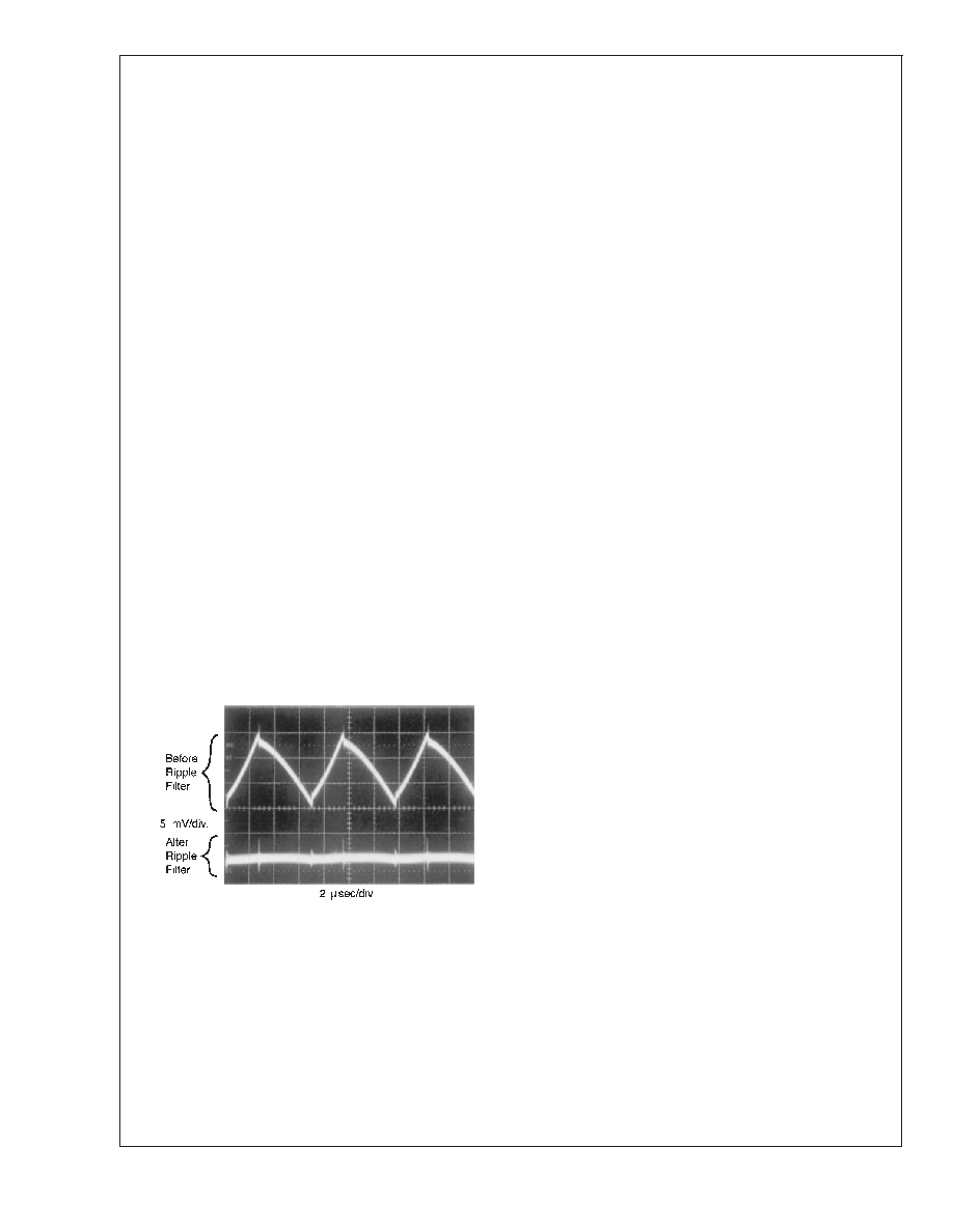
voltage is needed (less than 20 mV), a post ripple filter is
recommended. (See
Figure 1.) The inductance required is
typically between 1 H and 5 H, with low DC resistance, to
maintain good load regulation. A low ESR output filter ca-
pacitor is also required to assure good dynamic load re-
sponse and ripple reduction. The ESR of this capacitor may
be as low as desired, because it is out of the regulator
feedback loop. The photo shown in
Figure 17 shows a
typical output ripple voltage, with and without a post ripple
filter.
When observing output ripple with a scope, it is essential
that a short, low inductance scope probe ground connection
be used. Most scope probe manufacturers provide a special
probe terminator which is soldered onto the regulator board,
preferable at the output capacitor. This provides a very short
scope ground thus eliminating the problems associated with
the 3 inch ground lead normally provided with the probe, and
provides a much cleaner and more accurate picture of the
ripple voltage waveform.
The voltage spikes are caused by the fast switching action of
the output switch and the diode, and the parasitic inductance
of the output filter capacitor, and its associated wiring. To
minimize these voltage spikes, the output capacitor should
be designed for switching regulator applications, and the
lead lengths must be kept very short. Wiring inductance,
stray capacitance, as well as the scope probe used to evalu-
ate these transients, all contribute to the amplitude of these
spikes.
When a switching regulator is operating in the continuous
mode, the inductor current waveform ranges from a triangu-
lar to a sawtooth type of waveform (depending on the input
voltage). For a given input and output voltage, the
peak-to-peak amplitude of this inductor current waveform
remains constant. As the load current increases or de-
creases, the entire sawtooth current waveform also rises
and falls. The average value (or the center) of this current
waveform is equal to the DC load current.
If the load current drops to a low enough level, the bottom of
the sawtooth current waveform will reach zero, and the
switcher will smoothly change from a continuous to a discon-
tinuous mode of operation. Most switcher designs (irregard-
less how large the inductor value is) will be forced to run
discontinuous if the output is lightly loaded. This is a per-
fectly acceptable mode of operation.
01258332
FIGURE 17. Post Ripple Filter Waveform
LM2596
www.national.com
22
相关PDF资料 |
PDF描述 |
|---|---|
| LM4120AI5.0MWC | 1-OUTPUT THREE TERM VOLTAGE REFERENCE, 5 V, UUC |
| LQS100A48-1V2A | 1-OUTPUT 120 W DC-DC REG PWR SUPPLY MODULE |
| LEN-0.8/28-D12M | 1-OUTPUT 0.25 W DC-DC REG PWR SUPPLY MODULE |
| LEN-1/28-D12 | 1-OUTPUT 0.25 W DC-DC REG PWR SUPPLY MODULE |
| LEN-2/28-D12 | 1-OUTPUT 0.25 W DC-DC REG PWR SUPPLY MODULE |
相关代理商/技术参数 |
参数描述 |
|---|---|
| LM2596ADPBCKGEVB | 功能描述:BOARD EVAL LM2596ADJ BUCK D2PAK RoHS:是 类别:编程器,开发系统 >> 评估板 - DC/DC 与 AC/DC(离线)SMPS 系列:* 产品培训模块:Obsolescence Mitigation Program 标准包装:1 系列:True Shutdown™ 主要目的:DC/DC,步升 输出及类型:1,非隔离 功率 - 输出:- 输出电压:- 电流 - 输出:1A 输入电压:2.5 V ~ 5.5 V 稳压器拓扑结构:升压 频率 - 开关:3MHz 板类型:完全填充 已供物品:板 已用 IC / 零件:MAX8969 |
| LM2596ATPBCKGEVB | 功能描述:BOARD EVAL LM2596ADJ BUCK TO-220 RoHS:是 类别:编程器,开发系统 >> 评估板 - DC/DC 与 AC/DC(离线)SMPS 系列:* 产品培训模块:Obsolescence Mitigation Program 标准包装:1 系列:True Shutdown™ 主要目的:DC/DC,步升 输出及类型:1,非隔离 功率 - 输出:- 输出电压:- 电流 - 输出:1A 输入电压:2.5 V ~ 5.5 V 稳压器拓扑结构:升压 频率 - 开关:3MHz 板类型:完全填充 已供物品:板 已用 IC / 零件:MAX8969 |
| LM2596DSADJG | 功能描述:直流/直流开关调节器 3A BUCK SWCH 150KHZ RoHS:否 制造商:International Rectifier 最大输入电压:21 V 开关频率:1.5 MHz 输出电压:0.5 V to 0.86 V 输出电流:4 A 输出端数量: 最大工作温度: 安装风格:SMD/SMT 封装 / 箱体:PQFN 4 x 5 |
| LM2596DSADJR4G | 功能描述:直流/直流开关调节器 3A BUCK SWCH 150KHZ RoHS:否 制造商:International Rectifier 最大输入电压:21 V 开关频率:1.5 MHz 输出电压:0.5 V to 0.86 V 输出电流:4 A 输出端数量: 最大工作温度: 安装风格:SMD/SMT 封装 / 箱体:PQFN 4 x 5 |
| LM2596S | 制造商:Texas Instruments 功能描述: |
发布紧急采购,3分钟左右您将得到回复。