- 您现在的位置:买卖IC网 > PDF目录80315 > LM2596-3.3MWC (NATIONAL SEMICONDUCTOR CORP) 7.5 A SWITCHING REGULATOR, 173 kHz SWITCHING FREQ-MAX, UUC PDF资料下载
参数资料
| 型号: | LM2596-3.3MWC |
| 厂商: | NATIONAL SEMICONDUCTOR CORP |
| 元件分类: | 稳压器 |
| 英文描述: | 7.5 A SWITCHING REGULATOR, 173 kHz SWITCHING FREQ-MAX, UUC |
| 封装: | WAFER |
| 文件页数: | 32/36页 |
| 文件大小: | 827K |
| 代理商: | LM2596-3.3MWC |
第1页第2页第3页第4页第5页第6页第7页第8页第9页第10页第11页第12页第13页第14页第15页第16页第17页第18页第19页第20页第21页第22页第23页第24页第25页第26页第27页第28页第29页第30页第31页当前第32页第33页第34页第35页第36页
All Output Voltage Versions
Electrical Characteristics (Continued)
Specifications with standard type face are for T
J = 25C, and those with boldface type apply over full Operating Tempera-
ture Range. Unless otherwise specified, V
IN = 12V for the 3.3V, 5V, and Adjustable version and VIN = 24V for the 12V ver-
sion. I
LOAD = 500 mA
Symbol
Parameter
Conditions
LM2596-XX
Units
(Limits)
Typ
Limit
I
H
ON /OFF Pin Input Current
V
LOGIC = 2.5V (Regulator OFF)
5
A
15
A(max)
I
L
V
LOGIC = 0.5V (Regulator ON)
0.02
A
5
A(max)
Note 1: Absolute Maximum Ratings indicate limits beyond which damage to the device may occur. Operating Ratings indicate conditions for which the device is
intended to be functional, but do not guarantee specific performance limits. For guaranteed specifications and test conditions, see the Electrical Characteristics.
Note 2: The human body model is a 100 pF capacitor discharged through a 1.5k resistor into each pin.
Note 3: Typical numbers are at 25C and represent the most likely norm.
Note 4: All limits guaranteed at room temperature (standard type face) and at temperature extremes (bold type face). All room temperature limits are 100%
production tested. All limits at temperature extremes are guaranteed via correlation using standard Statistical Quality Control (SQC) methods. All limits are used to
calculate Average Outgoing Quality Level (AOQL).
Note 5: External components such as the catch diode, inductor, input and output capacitors, and voltage programming resistors can affect switching regulator
system performance. When the LM2596 is used as shown in the
Figure 1 test circuit, system performance will be as shown in system parameters section of Electrical
Characteristics.
Note 6: The switching frequency is reduced when the second stage current limit is activated.
Note 7: No diode, inductor or capacitor connected to output pin.
Note 8: Feedback pin removed from output and connected to 0V to force the output transistor switch ON.
Note 9: Feedback pin removed from output and connected to 12V for the 3.3V, 5V, and the ADJ. version, and 15V for the 12V version, to force the output transistor
switch OFF.
Note 10: VIN = 40V.
Note 11: Junction to ambient thermal resistance (no external heat sink) for the TO-220 package mounted vertically, with the leads soldered to a printed circuit board
with (1 oz.) copper area of approximately 1 in2.
Note 12: Junction to ambient thermal resistance with the TO-263 package tab soldered to a single printed circuit board with 0.5 in2 of (1 oz.) copper area.
Note 13: Junction to ambient thermal resistance with the TO-263 package tab soldered to a single sided printed circuit board with 2.5 in2 of (1 oz.) copper area.
Note 14: Junction to ambient thermal resistance with the TO-263 package tab soldered to a double sided printed circuit board with 3 in2 of (1 oz.) copper area on
the LM2596S side of the board, and approximately 16 in2 of copper on the other side of the p-c board. See Application Information in this data sheet and the thermal
model in Switchers Made Simple version 4.3 software.
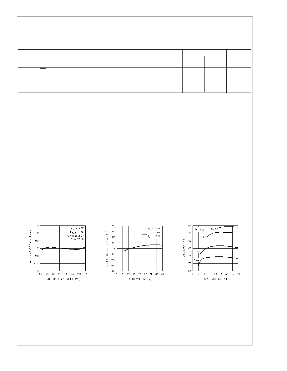
Typical Performance Characteristics (Circuit of Figure 1)
Normalized
Output Voltage
Line Regulation
Efficiency
01258304
01258305
01258306
LM2596
www.national.com
5
相关PDF资料 |
PDF描述 |
|---|---|
| LM4120AI5.0MWC | 1-OUTPUT THREE TERM VOLTAGE REFERENCE, 5 V, UUC |
| LQS100A48-1V2A | 1-OUTPUT 120 W DC-DC REG PWR SUPPLY MODULE |
| LEN-0.8/28-D12M | 1-OUTPUT 0.25 W DC-DC REG PWR SUPPLY MODULE |
| LEN-1/28-D12 | 1-OUTPUT 0.25 W DC-DC REG PWR SUPPLY MODULE |
| LEN-2/28-D12 | 1-OUTPUT 0.25 W DC-DC REG PWR SUPPLY MODULE |
相关代理商/技术参数 |
参数描述 |
|---|---|
| LM2596ADPBCKGEVB | 功能描述:BOARD EVAL LM2596ADJ BUCK D2PAK RoHS:是 类别:编程器,开发系统 >> 评估板 - DC/DC 与 AC/DC(离线)SMPS 系列:* 产品培训模块:Obsolescence Mitigation Program 标准包装:1 系列:True Shutdown™ 主要目的:DC/DC,步升 输出及类型:1,非隔离 功率 - 输出:- 输出电压:- 电流 - 输出:1A 输入电压:2.5 V ~ 5.5 V 稳压器拓扑结构:升压 频率 - 开关:3MHz 板类型:完全填充 已供物品:板 已用 IC / 零件:MAX8969 |
| LM2596ATPBCKGEVB | 功能描述:BOARD EVAL LM2596ADJ BUCK TO-220 RoHS:是 类别:编程器,开发系统 >> 评估板 - DC/DC 与 AC/DC(离线)SMPS 系列:* 产品培训模块:Obsolescence Mitigation Program 标准包装:1 系列:True Shutdown™ 主要目的:DC/DC,步升 输出及类型:1,非隔离 功率 - 输出:- 输出电压:- 电流 - 输出:1A 输入电压:2.5 V ~ 5.5 V 稳压器拓扑结构:升压 频率 - 开关:3MHz 板类型:完全填充 已供物品:板 已用 IC / 零件:MAX8969 |
| LM2596DSADJG | 功能描述:直流/直流开关调节器 3A BUCK SWCH 150KHZ RoHS:否 制造商:International Rectifier 最大输入电压:21 V 开关频率:1.5 MHz 输出电压:0.5 V to 0.86 V 输出电流:4 A 输出端数量: 最大工作温度: 安装风格:SMD/SMT 封装 / 箱体:PQFN 4 x 5 |
| LM2596DSADJR4G | 功能描述:直流/直流开关调节器 3A BUCK SWCH 150KHZ RoHS:否 制造商:International Rectifier 最大输入电压:21 V 开关频率:1.5 MHz 输出电压:0.5 V to 0.86 V 输出电流:4 A 输出端数量: 最大工作温度: 安装风格:SMD/SMT 封装 / 箱体:PQFN 4 x 5 |
| LM2596S | 制造商:Texas Instruments 功能描述: |
发布紧急采购,3分钟左右您将得到回复。