- 您现在的位置:买卖IC网 > PDF目录80315 > LM2596-3.3MWC (NATIONAL SEMICONDUCTOR CORP) 7.5 A SWITCHING REGULATOR, 173 kHz SWITCHING FREQ-MAX, UUC PDF资料下载
参数资料
| 型号: | LM2596-3.3MWC |
| 厂商: | NATIONAL SEMICONDUCTOR CORP |
| 元件分类: | 稳压器 |
| 英文描述: | 7.5 A SWITCHING REGULATOR, 173 kHz SWITCHING FREQ-MAX, UUC |
| 封装: | WAFER |
| 文件页数: | 18/36页 |
| 文件大小: | 827K |
| 代理商: | LM2596-3.3MWC |
第1页第2页第3页第4页第5页第6页第7页第8页第9页第10页第11页第12页第13页第14页第15页第16页第17页当前第18页第19页第20页第21页第22页第23页第24页第25页第26页第27页第28页第29页第30页第31页第32页第33页第34页第35页第36页
Application Information (Continued)
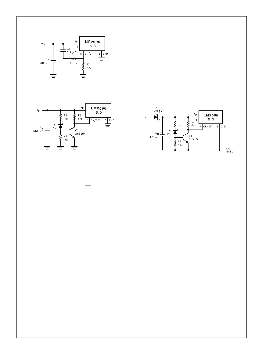
DELAYED STARTUP
The circuit in
Figure 21 uses the the ON /OFF pin to provide
a time delay between the time the input voltage is applied
and the time the output voltage comes up (only the circuitry
pertaining to the delayed start up is shown). As the input
voltage rises, the charging of capacitor C1 pulls the ON /OFF
pin high, keeping the regulator off. Once the input voltage
reaches its final value and the capacitor stops charging, and
resistor R
2 pulls the ON /OFF pin low, thus allowing the
circuit to start switching. Resistor R
1 is included to limit the
maximum voltage applied to the ON /OFF pin (maximum of
25V), reduces power supply noise sensitivity, and also limits
the capacitor, C1, discharge current. When high input ripple
voltage exists, avoid long delay time, because this ripple can
be coupled into the ON /OFF pin and cause problems.
This delayed startup feature is useful in situations where the
input power source is limited in the amount of current it can
deliver. It allows the input voltage to rise to a higher voltage
before the regulator starts operating. Buck regulators require
less input current at higher input voltages.
UNDERVOLTAGE LOCKOUT
Some applications require the regulator to remain off until
the input voltage reaches a predetermined voltage. An und-
ervoltage lockout feature applied to a buck regulator is
shown in
Figure 22, while Figure 23 and 24 applies the same
feature to an inverting circuit. The circuit in
Figure 23 fea-
tures a constant threshold voltage for turn on and turn off
(zener voltage plus approximately one volt). If hysteresis is
needed, the circuit in
Figure 24 has a turn ON voltage which
is different than the turn OFF voltage. The amount of hyster-
esis is approximately equal to the value of the output volt-
age. If zener voltages greater than 25V are used, an addi-
tional 47 k
resistor is needed from the ON /OFF pin to the
ground pin to stay within the 25V maximum limit of the ON
/OFF pin.
INVERTING REGULATOR
The circuit in
Figure 25 converts a positive input voltage to a
negative output voltage with a common ground. The circuit
operates by bootstrapping the regulator’s ground pin to the
negative output voltage, then grounding the feedback pin,
the regulator senses the inverted output voltage and regu-
lates it.
This example uses the LM2596-5.0 to generate a 5V out-
put, but other output voltages are possible by selecting other
output voltage versions, including the adjustable version.
Since this regulator topology can produce an output voltage
that is either greater than or less than the input voltage, the
maximum output current greatly depends on both the input
and output voltage. The curve shown in
Figure 26 provides a
guide as to the amount of output load current possible for the
different input and output voltage conditions.
The maximum voltage appearing across the regulator is the
absolute sum of the input and output voltage, and this must
be limited to a maximum of 40V. For example, when convert-
ing +20V to 12V, the regulator would see 32V between the
input pin and ground pin. The LM2596 has a maximum input
voltage spec of 40V.
Additional diodes are required in this regulator configuration.
Diode D1 is used to isolate input voltage ripple or noise from
coupling through the C
IN capacitor to the output, under light
or no load conditions. Also, this diode isolation changes the
topology to closley resemble a buck configuration thus pro-
viding good closed loop stability. A Schottky diode is recom-
mended for low input voltages, (because of its lower voltage
drop) but for higher input voltages, a fast recovery diode
could be used.
Without diode D3, when the input voltage is first applied, the
charging current of C
IN can pull the output positive by sev-
eral volts for a short period of time. Adding D3 prevents the
output from going positive by more than a diode voltage.
01258336
FIGURE 21. Delayed Startup
01258337
FIGURE 22. Undervoltage Lockout
for Buck Regulator
01258338
This circuit has an ON/OFF threshold of approximately 13V.
FIGURE 23. Undervoltage Lockout
for Inverting Regulator
LM2596
www.national.com
25
相关PDF资料 |
PDF描述 |
|---|---|
| LM4120AI5.0MWC | 1-OUTPUT THREE TERM VOLTAGE REFERENCE, 5 V, UUC |
| LQS100A48-1V2A | 1-OUTPUT 120 W DC-DC REG PWR SUPPLY MODULE |
| LEN-0.8/28-D12M | 1-OUTPUT 0.25 W DC-DC REG PWR SUPPLY MODULE |
| LEN-1/28-D12 | 1-OUTPUT 0.25 W DC-DC REG PWR SUPPLY MODULE |
| LEN-2/28-D12 | 1-OUTPUT 0.25 W DC-DC REG PWR SUPPLY MODULE |
相关代理商/技术参数 |
参数描述 |
|---|---|
| LM2596ADPBCKGEVB | 功能描述:BOARD EVAL LM2596ADJ BUCK D2PAK RoHS:是 类别:编程器,开发系统 >> 评估板 - DC/DC 与 AC/DC(离线)SMPS 系列:* 产品培训模块:Obsolescence Mitigation Program 标准包装:1 系列:True Shutdown™ 主要目的:DC/DC,步升 输出及类型:1,非隔离 功率 - 输出:- 输出电压:- 电流 - 输出:1A 输入电压:2.5 V ~ 5.5 V 稳压器拓扑结构:升压 频率 - 开关:3MHz 板类型:完全填充 已供物品:板 已用 IC / 零件:MAX8969 |
| LM2596ATPBCKGEVB | 功能描述:BOARD EVAL LM2596ADJ BUCK TO-220 RoHS:是 类别:编程器,开发系统 >> 评估板 - DC/DC 与 AC/DC(离线)SMPS 系列:* 产品培训模块:Obsolescence Mitigation Program 标准包装:1 系列:True Shutdown™ 主要目的:DC/DC,步升 输出及类型:1,非隔离 功率 - 输出:- 输出电压:- 电流 - 输出:1A 输入电压:2.5 V ~ 5.5 V 稳压器拓扑结构:升压 频率 - 开关:3MHz 板类型:完全填充 已供物品:板 已用 IC / 零件:MAX8969 |
| LM2596DSADJG | 功能描述:直流/直流开关调节器 3A BUCK SWCH 150KHZ RoHS:否 制造商:International Rectifier 最大输入电压:21 V 开关频率:1.5 MHz 输出电压:0.5 V to 0.86 V 输出电流:4 A 输出端数量: 最大工作温度: 安装风格:SMD/SMT 封装 / 箱体:PQFN 4 x 5 |
| LM2596DSADJR4G | 功能描述:直流/直流开关调节器 3A BUCK SWCH 150KHZ RoHS:否 制造商:International Rectifier 最大输入电压:21 V 开关频率:1.5 MHz 输出电压:0.5 V to 0.86 V 输出电流:4 A 输出端数量: 最大工作温度: 安装风格:SMD/SMT 封装 / 箱体:PQFN 4 x 5 |
| LM2596S | 制造商:Texas Instruments 功能描述: |
发布紧急采购,3分钟左右您将得到回复。