- 您现在的位置:买卖IC网 > PDF目录2082 > LMH6734MQX/NOPB (National Semiconductor)IC BUFFER TRPL SELECT 16-SSOP PDF资料下载
参数资料
| 型号: | LMH6734MQX/NOPB |
| 厂商: | National Semiconductor |
| 文件页数: | 9/21页 |
| 文件大小: | 0K |
| 描述: | IC BUFFER TRPL SELECT 16-SSOP |
| 标准包装: | 2,500 |
| 系列: | PowerWise® |
| 应用: | 电流反馈 |
| 电路数: | 3 |
| -3db带宽: | 925MHz |
| 转换速率: | 3750 V/µs |
| 电流 - 电源: | 19.5mA |
| 电流 - 输出 / 通道: | 80mA |
| 电压 - 电源,单路/双路(±): | 3 V ~ 12 V,±1.5 V ~ 6 V |
| 安装类型: | 表面贴装 |
| 封装/外壳: | 16-LSSOP(0.154",3.90mm 宽) |
| 供应商设备封装: | 16-QSOP |
| 包装: | 带卷 (TR) |
| 配用: | LMH730275/NOPB-ND - EVAL BOARD HS TRIPLE SSOP OPAMP |
| 其它名称: | LMH6734MQX |
+
-
RIN
50:
- V
+ V
ROUT
50:
CL
10 pF
RL
1 k:
VIN
0.1
10
FREQUENCY (MHz)
-20
-12
0
N
O
R
MAL
IZ
ED
G
AI
N
(
d
B
)
1000
100
1
-4
-8
-16
-2
-6
-10
-14
-18
L = 10 ft
L = 25 ft
L = 50 ft
L = 100 ft
L = 150 ft
L = 200 ft
V
+
= +5V
V
-
= -5V
VIN = 1 VPP
CAT5 LENGTH = L
OBSOLETE
SNOSAY0C – JUNE 2007 – REVISED APRIL 2013
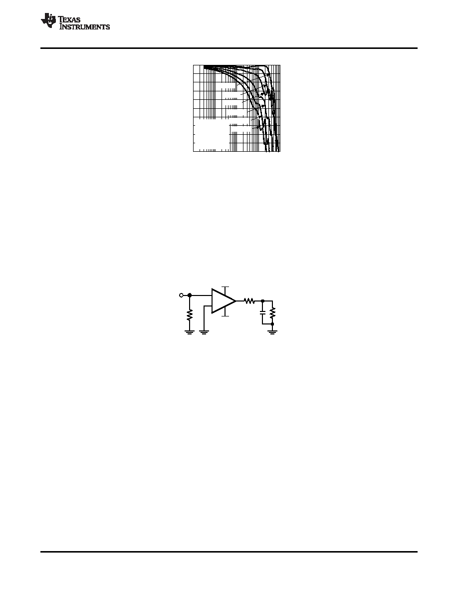
Figure 46. Frequency Response vs. Normalized Gain and CAT5 Cable Length
DRIVING CAPACITIVE LOADS
Capacitive output loading applications will benefit from the use of a series output resistor ROUT. Figure 47 shows
the use of a series output resistor, ROUT, to stabilize the amplifier output under capacitive loading. Capacitive
loads of 5 to 120 pF are the most critical, causing ringing, frequency response peaking and possible oscillation.
The charts “Suggested ROUT vs. Cap Load” give a recommended value for selecting a series output resistor for
mitigating capacitive loads. The values suggested in the charts are selected for 0.5 dB or less of peaking in the
frequency response. This gives a good compromise between settling time and bandwidth. For applications where
maximum frequency response is needed and some peaking is tolerable, the value of ROUT can be reduced
slightly from the recommended values.
Figure 47. Decoupling Capacitive Loads
LAYOUT CONSIDERATIONS
Whenever questions about layout arise, use the evaluation board as a guide. The LMH730275 is the evaluation
board supplied with samples of the LMH6734.
To reduce parasitic capacitances, ground and power planes should be removed near the input and output pins.
For long signal paths controlled impedance lines should be used, along with impedance matching elements at
both ends.
Bypass capacitors should be placed as close to the device as possible. Bypass capacitors from each rail to
ground are applied in pairs. The larger electrolytic bypass capacitors can be located farther from the device, the
smaller ceramic capacitors should be placed as close to the device as possible. The LMH6734 has multiple
power and ground pins for enhanced supply bypassing. Every pin should ideally have a separate bypass
capacitor. Sharing bypass capacitors may slightly degrade second order harmonic performance, especially if the
supply traces are thin and /or long. In Figure 35, Figure 36, and Figure 37 it is recommended an optional
capacitor, CSS= 0.01 μF, be connected between the split supplies for best second harmonic distortion. Another
option to using CSS is to use pairs of 0.01 μF and 0.1 μF ceramic capacitors for each supply bypass.
Copyright 2007–2013, Texas Instruments Incorporated
17
Product Folder Links: LMH6734
相关PDF资料 |
PDF描述 |
|---|---|
| LMK04010BISQ/NOPB | IC CLOCK CONDITIONER W/PLL 48LLP |
| LMV393MUTAG | IC OP AMP DUAL GP LV LV 8-UDFN |
| LMX339HASD+T | IC COMPARATOR GP QUAD 14-SOIC |
| LT1011AIS8#TRPBF | IC VOLTAGE COMPARATOR 5V 8-SOIC |
| LT1016IS8#TRPBF | IC COMPARATOR 10NS HI-SPD 8-SOIC |
相关代理商/技术参数 |
参数描述 |
|---|---|
| LMH6738 | 制造商:NSC 制造商全称:National Semiconductor 功能描述:Very Wideband, Low Distortion Triple Op Amp |
| LMH6738MQ | 功能描述:运算放大器 - 运放 RoHS:否 制造商:STMicroelectronics 通道数量:4 共模抑制比(最小值):63 dB 输入补偿电压:1 mV 输入偏流(最大值):10 pA 工作电源电压:2.7 V to 5.5 V 安装风格:SMD/SMT 封装 / 箱体:QFN-16 转换速度:0.89 V/us 关闭:No 输出电流:55 mA 最大工作温度:+ 125 C 封装:Reel |
| LMH6738MQ/NOPB | 功能描述:运算放大器 - 运放 Triple Video Op-Amp RoHS:否 制造商:STMicroelectronics 通道数量:4 共模抑制比(最小值):63 dB 输入补偿电压:1 mV 输入偏流(最大值):10 pA 工作电源电压:2.7 V to 5.5 V 安装风格:SMD/SMT 封装 / 箱体:QFN-16 转换速度:0.89 V/us 关闭:No 输出电流:55 mA 最大工作温度:+ 125 C 封装:Reel |
| LMH6738MQX | 功能描述:运算放大器 - 运放 RoHS:否 制造商:STMicroelectronics 通道数量:4 共模抑制比(最小值):63 dB 输入补偿电压:1 mV 输入偏流(最大值):10 pA 工作电源电压:2.7 V to 5.5 V 安装风格:SMD/SMT 封装 / 箱体:QFN-16 转换速度:0.89 V/us 关闭:No 输出电流:55 mA 最大工作温度:+ 125 C 封装:Reel |
| LMH6738MQX/NOPB | 功能描述:运算放大器 - 运放 RoHS:否 制造商:STMicroelectronics 通道数量:4 共模抑制比(最小值):63 dB 输入补偿电压:1 mV 输入偏流(最大值):10 pA 工作电源电压:2.7 V to 5.5 V 安装风格:SMD/SMT 封装 / 箱体:QFN-16 转换速度:0.89 V/us 关闭:No 输出电流:55 mA 最大工作温度:+ 125 C 封装:Reel |
发布紧急采购,3分钟左右您将得到回复。