- 您现在的位置:买卖IC网 > PDF目录16329 > LMK04031BEVAL/NOPB (National Semiconductor)EVAL BOARD LMK04031BISQ PDF资料下载
参数资料
| 型号: | LMK04031BEVAL/NOPB |
| 厂商: | National Semiconductor |
| 文件页数: | 18/65页 |
| 文件大小: | 0K |
| 描述: | EVAL BOARD LMK04031BISQ |
| 标准包装: | 1 |
| 系列: | PowerWise® |
| 主要目的: | 计时,多用途 |
| 嵌入式: | 否 |
| 已用 IC / 零件: | LMK04031 |
| 已供物品: | 板,线缆,文档,软件 |
第1页第2页第3页第4页第5页第6页第7页第8页第9页第10页第11页第12页第13页第14页第15页第16页第17页当前第18页第19页第20页第21页第22页第23页第24页第25页第26页第27页第28页第29页第30页第31页第32页第33页第34页第35页第36页第37页第38页第39页第40页第41页第42页第43页第44页第45页第46页第47页第48页第49页第50页第51页第52页第53页第54页第55页第56页第57页第58页第59页第60页第61页第62页第63页第64页第65页
Distribution
Path
SYNC*
CLKout0
CLKout1
CLKout2
SNOSAZ8J – SEPTEMBER 2008 – REVISED SEPTEMBER 2011
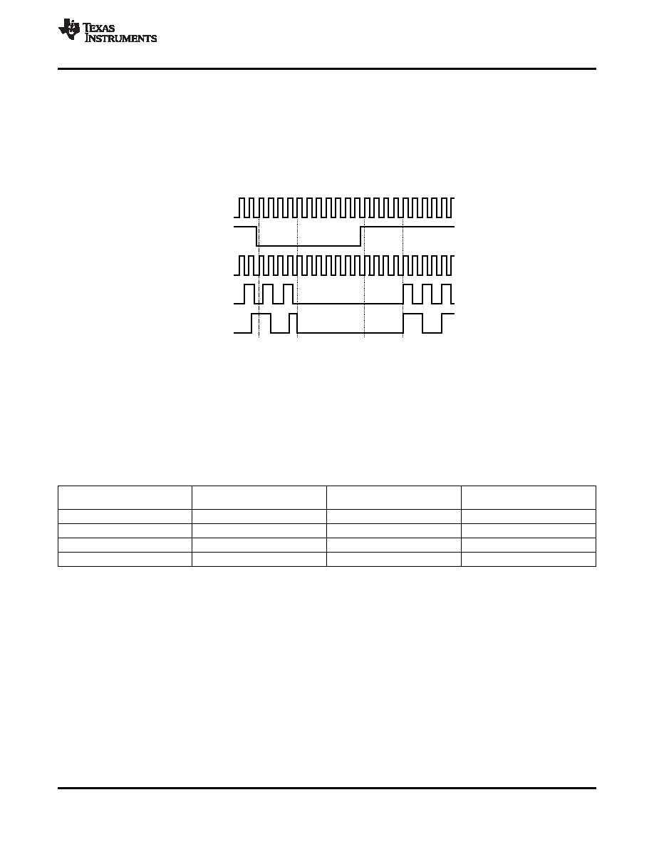
Global Clock Output Synchronization (Sync*)
The SYNC* input is used to synchronize the active clock outputs. When SYNC* is held in a logic low state, the
outputs are also held in a logic low state. When SYNC* goes high, the clock outputs are activated and will
transition to a high state simultaneously with one another.
SYNC* must be held low for greater than one clock cycle of the Clock Distribution Path. After this low event has
been registered, the outputs will not reflect the low state for four more cycles. Similarly after SYNC* becomes
high, the outputs will simultaneously transition high after four Clock Distribution Path cycles have passed. See
Figure 11 for further detail.
Figure 11. Clock Output synchronization using the SYNC* pin
Global Output Enable and Lock Detect
Each Clock Output Channel may be either enabled or put into a high impedance state via the Clock Output
Enable control bit (one for each channel). Each output enable control bit is gated with the Global Output Enable
input pin (GOE). The GOE pin provides an internal pull-up so that if it is un-terminated externally, then the clock
output states are determined by the Clock Channel Output Enable Register bits. All clock outputs can be
disabled simultaneously if the GOE pin is pulled low by an external signal.
Table 2. Clock Output Control
CLKoutX
EN_CLKout
CLKoutX Output State
GOE pin
_EN bit
_Global bit
1
Low
Don't care
0
Don't care
Off
0
Don't care
Off
1
High / No Connect
Enabled
The Lock Detect (LD) signal can be connected to the GOE pin in which case all outputs are disabled
automatically if the synthesizer is not locked. See EN_CLKoutX: Clock Channel Output Enable and also System
Level Diagram for actual implementation details.
The Lock Detect (LD) pin can be programmed to output a ‘High’ when both PLL1 and PLL2 are locked, or only
when PLL1 is locked or only when PLL2 is locked.
FUNCTIONAL DESCRIPTION
Architectural Overview
The LMK040xx chip consists of two high performance synthesizer blocks (Phase Locked Loop, internal
VCO/VCO Divider, and loop filter), source selection, distribution system, and independent clock output channels.
The Phase Frequency Detector in PLL1 compares the divided (R Divider 1) system clock signal from the
selected CLKinX and CLKinX* input with the divided (N Divider 1) output of the external VCXO attached to the
PLL2 OSCin port. The external loop filter for PLL1 should be narrow to provide an ultra clean reference clock
from the external VCXO to the OSCin/OSCin* pins for PLL2.
Copyright 2008–2011, Texas Instruments Incorporated
25
相关PDF资料 |
PDF描述 |
|---|---|
| LTC2903CS6-D1#TRMPBF | IC QUAD SPLY MONITOR ADJ SOT23-6 |
| 3-1906054-1 | CA 2MM OFNR 62.5/125,LC SEC GRE |
| PCV1V820MCL1GS | CAP ALUM 82UF 35V 20% SMD |
| 3-1906053-1 | CA 2MM OFNR 62.5/125,LC SEC YEL |
| LMK04033BEVAL/NOPB | BOARD EVALUATION LMK04033 |
相关代理商/技术参数 |
参数描述 |
|---|---|
| LMK04031BEVALXO | 功能描述:时钟和定时器开发工具 LMK04031 EVAL BOARD RoHS:否 制造商:Texas Instruments 产品:Evaluation Modules 类型:Clock Conditioners 工具用于评估:LMK04100B 频率:122.8 MHz 工作电源电压:3.3 V |
| LMK04031BISQ | 制造商:Texas Instruments 功能描述:Clock Conditioner 48-Pin LLP EP T/R |
| LMK04031BISQ/NOPB | 功能描述:时钟合成器/抖动清除器 RoHS:否 制造商:Skyworks Solutions, Inc. 输出端数量: 输出电平: 最大输出频率: 输入电平: 最大输入频率:6.1 GHz 电源电压-最大:3.3 V 电源电压-最小:2.7 V 封装 / 箱体:TSSOP-28 封装:Reel |
| LMK04031BISQE | 制造商:Texas Instruments 功能描述:PRECISION CLOCK CONDITIONER, 48LLP |
| LMK04031BISQE/NOPB | 功能描述:时钟合成器/抖动清除器 RoHS:否 制造商:Skyworks Solutions, Inc. 输出端数量: 输出电平: 最大输出频率: 输入电平: 最大输入频率:6.1 GHz 电源电压-最大:3.3 V 电源电压-最小:2.7 V 封装 / 箱体:TSSOP-28 封装:Reel |
发布紧急采购,3分钟左右您将得到回复。