参数资料
| 型号: | LT1169CS8 |
| 厂商: | Linear Technology |
| 文件页数: | 11/12页 |
| 文件大小: | 0K |
| 描述: | IC OPAMP JFET LONOISE DUAL 8SOIC |
| 标准包装: | 100 |
| 放大器类型: | J-FET |
| 电路数: | 2 |
| 转换速率: | 4.2 V/µs |
| 增益带宽积: | 5.3MHz |
| 电流 - 输入偏压: | 4pA |
| 电压 - 输入偏移: | 600µV |
| 电流 - 电源: | 5.3mA |
| 电压 - 电源,单路/双路(±): | ±4.5 V ~ 20 V |
| 工作温度: | 0°C ~ 70°C |
| 安装类型: | 表面贴装 |
| 封装/外壳: | 8-SOIC(0.154",3.90mm 宽) |
| 供应商设备封装: | 8-SO |
| 包装: | 管件 |
8
LT1169
U
S
A
O
PPLICATI
WU
U
I FOR ATIO
Figure 1. Comparison of LT1169, OP215, and AD822
Input Bias Current vs Common Mode Range
SOURCE RESISTANCE (
)
100
1
10
1k
10k
1k
100M
1G
LT1169 F02
100k
100
10M
10k
1M
INPUT
NOISE
VOLTAGE
(nV/
√
H
z)
Vn = AV √Vn
2
(OP AMP) + 4kTR + 2qIBR
2
SOURCE RESISTANCE = 2RS = R
* PLUS RESISTOR
PLUS RESISTOR 1000pF CAPACITOR
RESISTOR NOISE ONLY
LT1169
LT1124*
LT1124
LT1169
LT1124
LT1169*
–
+
CS
RS
VO
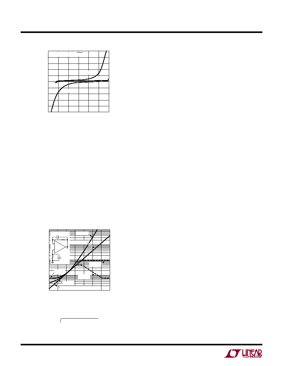
Figure 2. Comparison of LT1169 and LT1124 Total Output
1kHz Voltage Noise vs Source Resistance
the total noise. This means the LT1169 is superior to most
dual JFET op amps. Only the lowest noise bipolar op amps
have the advantage at low source resistances. As the
source resistance increases from 5k to 50k, the LT1169
will match the best bipolar op amps for noise perfor-
mance, since the thermal noise of the transducer (4kTR)
begins to dominate the total noise. A further increase in
source resistance, above 50k, is where the op amp’s
current noise component (2qIBR2) will eventually domi-
nate the total noise. At these high source resistances, the
LT1169 will out perform the lowest noise bipolar op amps
due to the inherently low current noise of FET input op
amps. Clearly, the LT1169 will extend the range of high
impedance transducers that can be used for high signal-
to-noise ratios. This makes the LT1169 the best choice for
high impedance, capacitive transducers.
Optimization Techniques for Charge Amplifiers
The high input impedance JFET front end makes the
LT1169 suitable in applications where very high charge
sensitivity is required. Figure 3 illustrates the LT1169 in its
inverting and noninverting modes of operation. A charge
amplifier is shown in the inverting mode example; the gain
depends on the principal of charge conservation at the
input of the LT1169. The charge across the transducer
capacitance CS is transferred to the feedback capacitor CF
resulting in a change in voltage dV, which is equal to dQ/CF.
The gain therefore is 1 + CF/CS. For unity-gain, the CF
should equal the transducer capacitance plus the input
capacitance of the LT1169 and RF should equal RS.
In the noninverting mode example, the transducer current
is converted to a change in voltage by the transducer
capacitance, CS. This voltage is then buffered by the
LT1169 with a gain of 1 + R1/R2. A DC path is provided by
RS, which is either the transducer impedance or an
external resistor. Since RS is usually several orders of
magnitude greater than the parallel combination of R1
and R2, RB is added to balance the DC offset caused by the
noninverting input bias current and RS. The input bias
currents, although small at room temperature, can create
significant errors over increasing temperature, especially
with transducer resistances of up to 1000M
or more.
The optimum value for RB is determined by equating the
thermal noise (4kTRS) to the current noise (2qIB) times
RS2. Solving for RS results in RB = RS = 2VT/IB. A parallel
Amplifying Signals from High Impedance Transducers
The low voltage and current noise offered by the LT1169
makes it useful in a wide range of applications, especially
where high impedance, capacitive transducers are used
such as hydrophones, precision accelerometers, and
photodiodes. The total output noise in such a system is
the gain times the RMS sum of the op amp’s input referred
voltage noise, the thermal noise of the transducer, and the
op amp’s input bias current noise times the transducer
impedance. Figure 2 shows total input voltage noise
versus source resistance. In a low source resistance
(< 5k) application the op amp voltage noise will dominate
COMMON MODE RANGE (V)
–15
–100
INPUT
BIAS
CURRENT
(pA)
–60
–40
–20
0
20
40
–10
–5
05
LT1169 F01
10
60
80
100
–80
15
LT1169
AD822
CURRENT NOISE =
√2qIB
OP215
相关PDF资料 |
PDF描述 |
|---|---|
| HMTSW-103-07-G-S-231 | CONN HEADER 3POS .25 GLD |
| ISL28006FHADJZ-T7A | IC AMP CURRENT SENSE SOT23-6 |
| LT1008IN8 | IC PREC OP-AMP UNIVRSL SNGL 8DIP |
| 961218-6804-AR | CONN HEADER VERT DUAL 18POS GOLD |
| LF398AN8 | IC AMP PREC SAMPLE & HOLD 8-DIP |
相关代理商/技术参数 |
参数描述 |
|---|---|
| LT1169CS8#PBF | 功能描述:IC OPAMP JFET LONOISE DUAL 8SOIC RoHS:是 类别:集成电路 (IC) >> Linear - Amplifiers - Instrumentation 系列:- 标准包装:2,500 系列:- 放大器类型:通用 电路数:4 输出类型:- 转换速率:0.6 V/µs 增益带宽积:1MHz -3db带宽:- 电流 - 输入偏压:45nA 电压 - 输入偏移:2000µV 电流 - 电源:1.4mA 电流 - 输出 / 通道:40mA 电压 - 电源,单路/双路(±):3 V ~ 32 V,±1.5 V ~ 16 V 工作温度:0°C ~ 70°C 安装类型:表面贴装 封装/外壳:14-TSSOP(0.173",4.40mm 宽) 供应商设备封装:14-TSSOP 包装:带卷 (TR) 其它名称:LM324ADTBR2G-NDLM324ADTBR2GOSTR |
| LT1169CS8#TR | 功能描述:IC OPAMP JFET DUAL LONOISE 8SOIC RoHS:否 类别:集成电路 (IC) >> Linear - Amplifiers - Instrumentation 系列:- 标准包装:73 系列:Over-The-Top® 放大器类型:通用 电路数:4 输出类型:满摆幅 转换速率:0.07 V/µs 增益带宽积:200kHz -3db带宽:- 电流 - 输入偏压:1nA 电压 - 输入偏移:285µV 电流 - 电源:50µA 电流 - 输出 / 通道:25mA 电压 - 电源,单路/双路(±):2 V ~ 44 V,±1 V ~ 22 V 工作温度:-40°C ~ 85°C 安装类型:表面贴装 封装/外壳:16-WFDFN 裸露焊盘 供应商设备封装:16-DFN-EP(5x3) 包装:管件 |
| LT1169CS8#TRPBF | 功能描述:IC OPAMP JFET LONOISE DUAL 8SOIC RoHS:是 类别:集成电路 (IC) >> Linear - Amplifiers - Instrumentation 系列:- 标准包装:2,500 系列:- 放大器类型:通用 电路数:1 输出类型:满摆幅 转换速率:0.11 V/µs 增益带宽积:350kHz -3db带宽:- 电流 - 输入偏压:4nA 电压 - 输入偏移:20µV 电流 - 电源:260µA 电流 - 输出 / 通道:20mA 电压 - 电源,单路/双路(±):2.7 V ~ 36 V,±1.35 V ~ 18 V 工作温度:-40°C ~ 85°C 安装类型:表面贴装 封装/外壳:8-SOIC(0.154",3.90mm 宽) 供应商设备封装:8-SO 包装:带卷 (TR) |
| LT117 | 制造商:LINER 制造商全称:Linear Technology 功能描述:Positive Adjustable Regulator |
| LT1170 | 制造商:LINER 制造商全称:Linear Technology 功能描述:100kHz, 5A, 2.5A and 1.25A High Efficiency Switching Regulators |
发布紧急采购,3分钟左右您将得到回复。