- 您现在的位置:买卖IC网 > PDF目录15245 > LT1339ISW#TRPBF (Linear Technology)IC REG CTRLR BST PWM CM 20-SOIC PDF资料下载
参数资料
| 型号: | LT1339ISW#TRPBF |
| 厂商: | Linear Technology |
| 文件页数: | 10/20页 |
| 文件大小: | 0K |
| 描述: | IC REG CTRLR BST PWM CM 20-SOIC |
| 标准包装: | 1,000 |
| PWM 型: | 电流模式 |
| 输出数: | 1 |
| 频率 - 最大: | 150kHz |
| 占空比: | 90% |
| 电源电压: | 最高 60V |
| 降压: | 无 |
| 升压: | 是 |
| 回扫: | 无 |
| 反相: | 无 |
| 倍增器: | 无 |
| 除法器: | 无 |
| Cuk: | 无 |
| 隔离: | 无 |
| 工作温度: | -40°C ~ 85°C |
| 封装/外壳: | 20-SOIC(0.295",7.50mm 宽) |
| 包装: | 带卷 (TR) |
�� �
�
�LT1339�
�APPLICATIO� N� S� I� N� FOR� M� ATIO� N�
�R� SENSE� Selection� for� Output� Current�
�R� SENSE� generates� a� voltage� that� is� proportional� to� the�
�inductor� current� for� use� by� the� LT1339� current� sense�
�amplifier.� The� value� of� R� SENSE� is� based� on� the� required�
�load� current.� The� average� current� limit� function� has� a�
�typical� threshold� of� 120mV/R� SENSE� ,� or:�
�R� SENSE� =� 120mV/I� LIMIT�
�Operation� with� V� SENSE� common� mode� voltage� below� 4.5V�
�may� slightly� degrade� current� limit� accuracy.� See� Average�
�Current� Limit� Threshold� Tolerance� vs� Common� Mode�
�Voltage� curve� in� the� Typical� Performance� Characteristics�
�section� for� more� information.�
�the� minimum� off-time� of� the� PWM� controller.� This� limits�
�maximum� duty� cycle� (DC� MAX� )� to:�
�DC� MAX� =� 1� –� (t� DISCH� )(f� O� )�
�This� relation� corresponds� to� the� minimum� value� of� the�
�timing� resistor� (R� CT� ),� which� can� be� determined� according�
�to� the� following� relation� (R� CT� vs� DC� MAX� graph� appears� in�
�the� Typical� Performance� Characteristics� section):�
�R� CT(MIN)� ≈� [(0.8)(10� –3� )(1� –� DC� MAX� )]� –1�
�Values� for� R� CT� >� 15k� yield� maximum� duty� cycles� above�
�90%.� Given� a� timing� resistor� value,� the� value� of� the� timing�
�capacitor� (C� CT� )� can� then� be� determined� for� desired� oper-�
�ating� frequency� (f� O� )� using� the� relation:�
�(� 1� /� f� O� )� ?� (� )� ??� 10� ?� 9� ??�
�(� R� CT� /� 1� .� 85� )� +�
�Output Voltage Programming�
�Output� voltage� is� programmed� through� a� resistor� feed-�
�back� network� to� V� FB� (Pin� 9)� on� the� LT1339.� This� pin� is� the�
�inverting� input� of� the� error� amplifier,� which� is� internally�
�referenced� to� 1.25V.� The� divider� is� ratioed� to� provide�
�1.25V� at� the� V� FB� pin� when� the� output� is� at� its� desired� value.�
�C� CT� ≈�
�100�
�1� .� 75�
�(� 2� .� 5� )� ??� 10� ?� 3� ??� ?� (� 3� .� 375� /� R� CT� )�
�The� output� voltage� is� thus� set� following� the� relation:�
�V� OUT� =� 1.25(1� +� R2/R1)�
�when� an� external� resistor� divider� is� connected� to� the�
�output� as� shown� in� Figure� 1.�
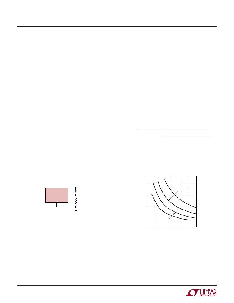
�A� plot� of� Operating� Frequency� vs� R� CT� and� C� CT� is� shown� in�
�Figure� 2.� Typical� 100kHz� operational� values� are� C� CT� =�
�1000pF� and� R� CT� =� 16.9k.�
�160�
�V� OUT�
�140�
�C� CT� = 1.0nF�
�LT1339� V� FB�
�SGND�
�9�
�R2�
�R1�
�120�
�100�
�80�
�C� CT� = 1.5nF�
�8�
�60�
�1339� ?� F01�
�Figure� 1.� Programming� LT1339� Output� Voltage�
�40�
�20�
�C� CT� = 3.3nF�
�C� CT� = 2.2nF�
�If� high� value� feedback� resistors� are� used,� the� input� bias�
�current� of� the� V� FB� pin� (1� μ� A� maximum)� could� cause� a� slight�
�0�
�0�
�5�
�10� 15� 20�
�TIMING� RESISTOR� (k� ?� )�
�25�
�30�
�increase� in� output� voltage.� A� Thevenin� resistance� at� the�
�V� FB� pin� of� <5k� is� recommended.�
�Oscillator� Components� R� CT� and� C� CT�
�The� LT1339� oscillator� creates� a� modified� sawtooth� wave�
�at� its� timing� node� (CT)� with� a� slow� charge,� rapid� discharge�
�characteristic.� The� rapid� discharge� time� corresponds� to�
�LT1339� ?� F02�
�Figure� 2.� Oscillator� Frequency� vs� R� CT� ,� C� CT�
�Average� Current� Limit�
�The� average� current� limit� function� is� implemented� using�
�an� external� capacitor� (C� AVG� )� connected� from� I� AVG� to� SGND�
�that� forms� a� single� pole� integrator� with� the� 50k� ?� output�
�sn1339� 1339fas�
�10�
�相关PDF资料 |
PDF描述 |
|---|---|
| SDR2207-561KL | INDUCTOR 560UH 800MA SMD |
| EBA36DTMT | CONN EDGECARD 72POS R/A .125 SLD |
| SDR2207-471KL | INDUCTOR 470UH 800MA SMD |
| LT1339ISW#TR | IC REG CTRLR BST PWM CM 20-SOIC |
| SDR2207-391KL | INDUCTOR 390UH 900MA SMD |
相关代理商/技术参数 |
参数描述 |
|---|---|
| LT133X1-104 | 制造商:未知厂家 制造商全称:未知厂家 功能描述:18+18 Dual channel 5V LVDS |
| LT1341 | 制造商:LINER 制造商全称:Linear Technology 功能描述:5V RS232 Transceiver with One Receiver Active in Shutdown |
| LT1341C | 制造商:LINER 制造商全称:Linear Technology 功能描述:5V RS232 Transceiver with One Receiver Active in Shutdown |
| LT1341CG | 功能描述:IC TXRX 5V RS232 W/SHTDWN 28SSOP RoHS:否 类别:集成电路 (IC) >> 接口 - 驱动器,接收器,收发器 系列:- 标准包装:27 系列:- 类型:收发器 驱动器/接收器数:3/3 规程:RS232,RS485 电源电压:4.75 V ~ 5.25 V 安装类型:表面贴装 封装/外壳:28-SOIC(0.295",7.50mm 宽) 供应商设备封装:28-SOIC 包装:管件 |
| LT1341CG#PBF | 功能描述:IC TXRX 5V RS232 W/SHTDWN 28SSOP RoHS:是 类别:集成电路 (IC) >> 接口 - 驱动器,接收器,收发器 系列:- 标准包装:27 系列:- 类型:收发器 驱动器/接收器数:3/3 规程:RS232,RS485 电源电压:4.75 V ~ 5.25 V 安装类型:表面贴装 封装/外壳:28-SOIC(0.295",7.50mm 宽) 供应商设备封装:28-SOIC 包装:管件 |
发布紧急采购,3分钟左右您将得到回复。