- 您现在的位置:买卖IC网 > PDF目录15245 > LT1339ISW#TRPBF (Linear Technology)IC REG CTRLR BST PWM CM 20-SOIC PDF资料下载
参数资料
| 型号: | LT1339ISW#TRPBF |
| 厂商: | Linear Technology |
| 文件页数: | 14/20页 |
| 文件大小: | 0K |
| 描述: | IC REG CTRLR BST PWM CM 20-SOIC |
| 标准包装: | 1,000 |
| PWM 型: | 电流模式 |
| 输出数: | 1 |
| 频率 - 最大: | 150kHz |
| 占空比: | 90% |
| 电源电压: | 最高 60V |
| 降压: | 无 |
| 升压: | 是 |
| 回扫: | 无 |
| 反相: | 无 |
| 倍增器: | 无 |
| 除法器: | 无 |
| Cuk: | 无 |
| 隔离: | 无 |
| 工作温度: | -40°C ~ 85°C |
| 封装/外壳: | 20-SOIC(0.295",7.50mm 宽) |
| 包装: | 带卷 (TR) |
�� �
�
�LT1339�
�APPLICATIO� N� S� I� N� FOR� M� ATIO� N�
�further� increasing� the� effective� compensation� slope� up� to�
�2�
�5V� REF�
�20%� for� a� given� setting.�
�Design� Example:�
�V� IN� =� 20V�
�R� SL1�
�45k�
�R� SL2�
�30k�
�4�
�LT1339�
�SL/ADJ�
�1339� ?� F07a�
�V� OUT� =� 15V� (DC� =� 0.75)�
�R� SENSE� =� 0.01� ?�
�f� O� =� 100kHz�
�L� =� 5� μ� H�
�The� minimum� inductor� usable� with� no� additional� slope�
�compensation� is:�
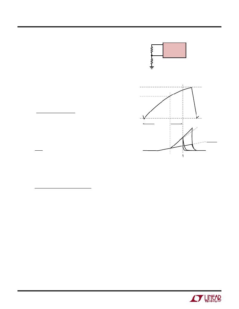
�Figure� 7a.� External� Slope� Compensation� Resistors�
�2.5V�
�2V�
�(� )� V� (� )� ?� (� )� 1� ?� =� 11� .� 9� μ� H�
�L� MIN� ≥�
�20� 0� .� 01� 1� .� 5�
�(� 0� .� 084� )(� 100000� )�
�0.8V�
�Since� L� =� 5� μ� H� is� less� than� L� MIN� ,� additional� slope� compen-�
�sation� is� necessary.� The� total� slope� compensation�
�required� is:�
�DC� =� 0.75�
�(0.084 + 0.139)(f� O� )�
�R� SENSE�
�(0.084)(f� O� )�
�(�
�)� ()�
�?� 20� V� ?�
�S� X� ≥� ?�
�?� 1� .� 5� ?� 1� =� 2� ?� 10� ?�
�?� 5� μ� H� ?�
�?� 6� ?�
�Amp/s�
�1339� ?� F07b�
�R� SENSE�
�(� )(� f� O� )�
�(� 2� )� ?� ?� (� SENSE� )� ?� (� 0� .� 084� )(� f� O� )�
�?� 10� 6� ?� R�
�Subtracting the internally generated slope compensation�
�and� solving� for� the� required� effective� resistance� at� SL/ADJ�
�yields:�
�2500�
�R� EQ� ≤� =� 21� .� 5� k�
�Setting� the� resistor� divider� reference� voltage� at� 2V� assures�
�that� the� additional� compensation� waveform� will� be�
�enabled� at� 75%� duty� cycle.� As� shown� in� Figure� 7a,� using�
�R� SL1� =� 45k� and� R� SL2� =� 30k� sets� the� desired� reference�
�voltage� and� has� a� R� EQ� of� 18k,� which� meets� both� design�
�requirements.� Figure� 7b� shows� the� slope� compensation�
�effective� waveforms� both� with� and� without� the� SL/ADJ�
�external� resistors.�
�Power� MOSFET� and� Catch� Diode� Selection�
�External� N-channel� MOSFET� switches� are� used� with� the�
�LT1339.� The� positive� gate-source� drive� voltage� of� the�
�LT1339� for� both� switches� is� roughly� equivalent� to� the�
�12V� IN� supply� voltage,� so� standard� threshold� MOSFETs�
�can� be� used.�
�Figure� 7b.� Slope� Compensation� Waveforms�
�Selection� criteria� for� the� power� MOSFETs� include� the� “ON”�
�resistance� (R� DS(ON)� ),� reverse� transfer� capacitance� (C� RSS� ),�
�maximum� drain-source� voltage� (V� DSS� )� and� maximum�
�output� current.�
�The� power� FETs� selected� must� have� a� maximum� operating�
�V� DSS� exceeding� the� maximum� V� IN� .� V� GS� voltage� maximum�
�must� exceed� the� 12V� IN� supply� voltage.�
�Once� voltage� requirements� have� been� determined,� R� DS(ON)�
�can� be� selected� based� on� allowable� power� dissipation� and�
�required� output� current.�
�In� an� LT1339� buck� converter,� the� average� inductor� current�
�is� equal� to� the� DC� load� current.� The� average� currents�
�through� the� main� and� synchronous� switches� are:�
�I� MAIN� =� (I� LOAD� )(DC)�
�I� SYNC� =� (I� LOAD� )(1� –� DC)�
�The� R� DS(ON)� required� for� a� given� conduction� loss� can� be�
�calculated� using� the� relation:�
�P� LOSS� =� (I� SWITCH� )� 2� (R� DS(ON)� )�
�sn1339� 1339fas�
�14�
�相关PDF资料 |
PDF描述 |
|---|---|
| SDR2207-561KL | INDUCTOR 560UH 800MA SMD |
| EBA36DTMT | CONN EDGECARD 72POS R/A .125 SLD |
| SDR2207-471KL | INDUCTOR 470UH 800MA SMD |
| LT1339ISW#TR | IC REG CTRLR BST PWM CM 20-SOIC |
| SDR2207-391KL | INDUCTOR 390UH 900MA SMD |
相关代理商/技术参数 |
参数描述 |
|---|---|
| LT133X1-104 | 制造商:未知厂家 制造商全称:未知厂家 功能描述:18+18 Dual channel 5V LVDS |
| LT1341 | 制造商:LINER 制造商全称:Linear Technology 功能描述:5V RS232 Transceiver with One Receiver Active in Shutdown |
| LT1341C | 制造商:LINER 制造商全称:Linear Technology 功能描述:5V RS232 Transceiver with One Receiver Active in Shutdown |
| LT1341CG | 功能描述:IC TXRX 5V RS232 W/SHTDWN 28SSOP RoHS:否 类别:集成电路 (IC) >> 接口 - 驱动器,接收器,收发器 系列:- 标准包装:27 系列:- 类型:收发器 驱动器/接收器数:3/3 规程:RS232,RS485 电源电压:4.75 V ~ 5.25 V 安装类型:表面贴装 封装/外壳:28-SOIC(0.295",7.50mm 宽) 供应商设备封装:28-SOIC 包装:管件 |
| LT1341CG#PBF | 功能描述:IC TXRX 5V RS232 W/SHTDWN 28SSOP RoHS:是 类别:集成电路 (IC) >> 接口 - 驱动器,接收器,收发器 系列:- 标准包装:27 系列:- 类型:收发器 驱动器/接收器数:3/3 规程:RS232,RS485 电源电压:4.75 V ~ 5.25 V 安装类型:表面贴装 封装/外壳:28-SOIC(0.295",7.50mm 宽) 供应商设备封装:28-SOIC 包装:管件 |
发布紧急采购,3分钟左右您将得到回复。