参数资料
| 型号: | LT1619ES8#PBF |
| 厂商: | Linear Technology |
| 文件页数: | 12/20页 |
| 文件大小: | 0K |
| 描述: | IC REG CTRLR PWM CM 8-SOIC |
| 标准包装: | 100 |
| PWM 型: | 电流模式 |
| 输出数: | 1 |
| 频率 - 最大: | 500kHz |
| 占空比: | 92% |
| 电源电压: | 1.9 V ~ 18 V |
| 降压: | 无 |
| 升压: | 是 |
| 回扫: | 是 |
| 反相: | 无 |
| 倍增器: | 无 |
| 除法器: | 无 |
| Cuk: | 是 |
| 隔离: | 是 |
| 工作温度: | -40°C ~ 85°C |
| 封装/外壳: | 8-SOIC(0.154",3.90mm 宽) |
| 包装: | 管件 |
| 产品目录页面: | 1328 (CN2011-ZH PDF) |
�� �
�
�LT1619�
�APPLICATIO� S� I� FOR� ATIO�
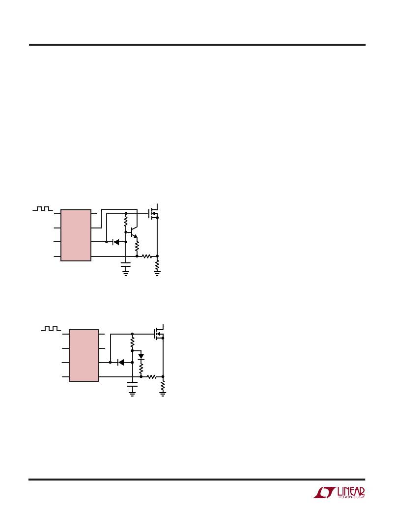
�Increasing� Ramp� Compensation� While� Synchronizing�
�The� LT1619� is� synchronized� by� forced� discharge� of� the�
�internal� timing� ramp.� The� timing� ramp� amplitude� de-�
�creases� as� the� synchronization� frequency� increases.� Since�
�the� internal� compensation� ramp� is� derived� from� the� timing�
�ramp,� reduced� timing� ramp� results� in� diminished� com-�
�pensating� ramp.� If� the� LT1619� is� synchronized� at� frequen-�
�cies� 20%� to� 30%� higher� than� the� free-running� frequency,�
�external� ramp� compensation� will� be� required.� Figures� 12�
�and� 13� show� two� such� schemes.�
�In� both� figures� the� compensating� ramps� are� kept� linear� by�
�making� R11-C1� and� R14-C2� products� substantially� higher�
�than� the� synchronizing� period.� The� compensation� ramps,�
�whose� peak� amplitudes� are� made� between� 1/4� to� 1/3� of� the�
�current� limit� threshold,� are� developed� across� R13.� As� a�
�result,� the� effective� current� limit� threshold� is� reduced� by�
�the� sum� of� the� compensating� ramp� and� the� offset� voltage�
�developed� across� R13� due� to� the� SENSE� pin� input� bias�
�current� (see� Figure� 5).� Moreover,� the� current� limit� thresh-�
�old� becomes� duty� cycle� dependent.�
�PC� Board� Layout� and� Other� Practical� Considerations�
�The� following� is� recommended� for� PC� board� layout:�
�1.� Trace� lengths� of� the� branches� carrying� switched� cur-�
�rent� should� be� kept� short.� For� example,� in� the� boost�
�converter� of� Figure� 1,� the� circuit� loop� formed� by� M1,�
�R� SENSE� ,� D1� and� C� OUT� carries� switched� current.� The� size�
�CLK�
�1�
�2�
�3�
�4�
�S/S� V� IN�
�FB� DRV�
�LT1619�
�V� C� GATE�
�GND� SENSE�
�8�
�7�
�6�
�5�
�R11�
�100k�
�D2�
�1N4148�
�Q1�
�2N2222�
�R12�
�2200� ?�
�MAIN� POWER�
�TRANSISTOR�
�of� this� loop� must� be� minimized.� R� SENSE� and� C� OUT�
�should� be� grounded� to� a� single� point� on� a� large� ground�
�plane.� This� reduces� switching� noise� and� overall� con-�
�verter� jitter.� It� is� also� preferable� to� ground� the� input�
�capacitor� C1� close� to� the� common� point� between� C� OUT�
�and� R� SENSE� although� this� is� less� important.�
�C1�
�220pF�
�R13�
�51� ?�
�R� SENSE�
�1619� F12�
�2.� Keep� the� trace� between� the� sense� resistor� and� the�
�SENSE� pin� short.� When� sensing� high� switch� current,�
�Kelvin� connection� to� R� SENSE� is� necessary.�
�Figure� 12.� Increasing� Ramp� Compensation.� Q1� Buffers� the� C1�
�Ramp.� D2� Discharges� C1.� Values� Shown� are� for� 10V� Gate� Drive�
�and� 15mV� Ramp� Across� R13� at� 90%� Duty� Cycle� and� 500kHz�
�3.� Bypass� both� the� V� IN� and� DRV� pins� with� ceramic� capaci-�
�tors� next� to� the� IC� and� the� ground� plane.�
�4.� Keep� high� voltage� switching� nodes,� such� as� the� drain�
�CLK�
�1�
�2�
�3�
�4�
�S/S� V� IN�
�FB� DRV�
�LT1619�
�V� C� GATE�
�GND� SENSE�
�8�
�7�
�6�
�5�
�D2�
�1N4148�
�C2�
�2.2nF�
�R14�
�8200� ?�
�D3�
�1N4148�
�R15�
�2400� ?�
�R13�
�51� ?�
�R� SENSE�
�and� gate� of� the� MOSFET,� away� from� the� FB� and� V� C� pins.�
�5.� Use� inductor� so� that� its� ripple� current� is� between� 1/4�
�and� 1/3� of� its� peak� current.� Steeper� inductor� current�
�ramp� results� in� sharper� PWM� comparator� switching,�
�hence� less� jitter.�
�6.� In� most� cases,� filtering� the� current� sense� signal� is� not�
�necessary� for� jitter-free� operation.�
�1619� F13�
�Figure� 14� is� the� PC� board� layout� for� the� 5V/8A� and� 12V/5A�
�Figure� 13.� Externally� Increasing� Ramp� Compensation.� Similar�
�boost� converters� shown� in� Figures� 15a� and� 16a.�
�to� Figure� 12� Except� That� C2� is� Not� Buffered� with� Transistor�
�1619fa�
�12�
�相关PDF资料 |
PDF描述 |
|---|---|
| ABC13DRXI-S734 | CONN EDGECARD 26POS DIP .100 SLD |
| ABC17DRTH-S734 | CONN EDGECARD 34POS DIP .100 SLD |
| LTC3851EUD#PBF | IC REG CTRLR BUCK PWM CM 16-QFN |
| RCA24DTAD | CONN EDGECARD 48POS R/A .125 SLD |
| RCA28DRMS | CONN EDGECARD 56POS .125 SQ WW |
相关代理商/技术参数 |
参数描述 |
|---|---|
| LT1620 | 制造商:LINER 制造商全称:Linear Technology 功能描述:Rail-to-Rail Current Sense Amplifier |
| LT1620CGN | 功能描述:IC AMP R-R CURRENT SENSE 16-SSOP RoHS:否 类别:集成电路 (IC) >> Linear - Amplifiers - Instrumentation 系列:- 标准包装:50 系列:- 放大器类型:通用 电路数:2 输出类型:满摆幅 转换速率:1.8 V/µs 增益带宽积:6.5MHz -3db带宽:4.5MHz 电流 - 输入偏压:5nA 电压 - 输入偏移:100µV 电流 - 电源:65µA 电流 - 输出 / 通道:35mA 电压 - 电源,单路/双路(±):1.8 V ~ 5.25 V,±0.9 V ~ 2.625 V 工作温度:-40°C ~ 85°C 安装类型:表面贴装 封装/外壳:10-TFSOP,10-MSOP(0.118",3.00mm 宽) 供应商设备封装:10-MSOP 包装:管件 |
| LT1620CGN#PBF | 功能描述:IC AMP R-R CURRENT SENSE 16-SSOP RoHS:是 类别:集成电路 (IC) >> Linear - Amplifiers - Instrumentation 系列:- 标准包装:50 系列:- 放大器类型:通用 电路数:2 输出类型:满摆幅 转换速率:1.8 V/µs 增益带宽积:6.5MHz -3db带宽:4.5MHz 电流 - 输入偏压:5nA 电压 - 输入偏移:100µV 电流 - 电源:65µA 电流 - 输出 / 通道:35mA 电压 - 电源,单路/双路(±):1.8 V ~ 5.25 V,±0.9 V ~ 2.625 V 工作温度:-40°C ~ 85°C 安装类型:表面贴装 封装/外壳:10-TFSOP,10-MSOP(0.118",3.00mm 宽) 供应商设备封装:10-MSOP 包装:管件 |
| LT1620CGN#TR | 功能描述:IC AMP CURRENT SENSE R-R 16SSOP RoHS:否 类别:集成电路 (IC) >> Linear - Amplifiers - Instrumentation 系列:- 标准包装:50 系列:LinCMOS™ 放大器类型:通用 电路数:4 输出类型:- 转换速率:0.05 V/µs 增益带宽积:110kHz -3db带宽:- 电流 - 输入偏压:0.7pA 电压 - 输入偏移:210µV 电流 - 电源:57µA 电流 - 输出 / 通道:30mA 电压 - 电源,单路/双路(±):3 V ~ 16 V,±1.5 V ~ 8 V 工作温度:-40°C ~ 85°C 安装类型:表面贴装 封装/外壳:14-SOIC(0.154",3.90mm 宽) 供应商设备封装:14-SOIC 包装:管件 产品目录页面:865 (CN2011-ZH PDF) 其它名称:296-1834296-1834-5 |
| LT1620CGN#TRPBF | 功能描述:IC AMP R-R CURRENT SENSE 16-SSOP RoHS:是 类别:集成电路 (IC) >> Linear - Amplifiers - Instrumentation 系列:- 标准包装:50 系列:LinCMOS™ 放大器类型:通用 电路数:4 输出类型:- 转换速率:0.05 V/µs 增益带宽积:110kHz -3db带宽:- 电流 - 输入偏压:0.7pA 电压 - 输入偏移:210µV 电流 - 电源:57µA 电流 - 输出 / 通道:30mA 电压 - 电源,单路/双路(±):3 V ~ 16 V,±1.5 V ~ 8 V 工作温度:-40°C ~ 85°C 安装类型:表面贴装 封装/外壳:14-SOIC(0.154",3.90mm 宽) 供应商设备封装:14-SOIC 包装:管件 产品目录页面:865 (CN2011-ZH PDF) 其它名称:296-1834296-1834-5 |
发布紧急采购,3分钟左右您将得到回复。