- 您现在的位置:买卖IC网 > PDF目录79915 > LT1871IMS-7#TR (LINEAR TECHNOLOGY CORP) SWITCHING CONTROLLER, 1000 kHz SWITCHING FREQ-MAX, PDSO10 PDF资料下载
参数资料
| 型号: | LT1871IMS-7#TR |
| 厂商: | LINEAR TECHNOLOGY CORP |
| 元件分类: | 稳压器 |
| 英文描述: | SWITCHING CONTROLLER, 1000 kHz SWITCHING FREQ-MAX, PDSO10 |
| 封装: | PLASTIC, MSOP-10 |
| 文件页数: | 2/32页 |
| 文件大小: | 461K |
| 代理商: | LT1871IMS-7#TR |
第1页当前第2页第3页第4页第5页第6页第7页第8页第9页第10页第11页第12页第13页第14页第15页第16页第17页第18页第19页第20页第21页第22页第23页第24页第25页第26页第27页第28页第29页第30页第31页第32页
LTC1871-7
10
18717fc
external frequency (above 1.3fO) can result in inadequate
slope compensation and possible subharmonic oscillation
(or jitter).
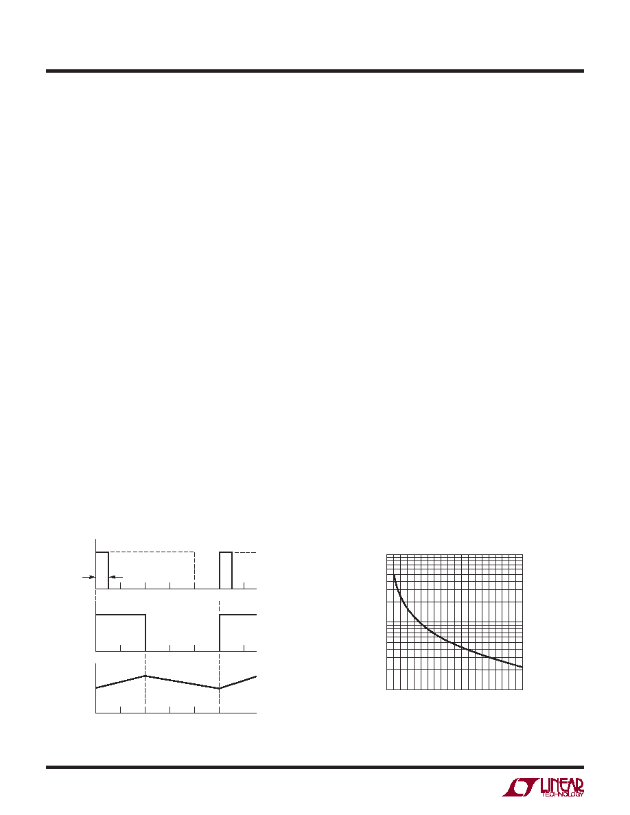
The external clock signal must exceed 2V for at least 25ns,
and should have a maximum duty cycle of 80%, as shown
in Figure 5. The MOSFET turn on will synchronize to the
rising edge of the external clock signal.
Programming the Operating Frequency
The choice of operating frequency and inductor value is
a tradeoff between efciency and component size. Low
frequency operation improves efciency by reducing
MOSFET and diode switching losses. However, lower
frequency operation requires more inductance for a given
amount of load current.
The LTC1871-7 uses a constant frequency architecture that
can be programmed over a 50kHz to 1000kHz range with
a single external resistor from the FREQ pin to ground, as
shown in Figure 1. The nominal voltage on the FREQ pin is
0.6V, and the current that ows into the FREQ pin is used
to charge and discharge an internal oscillator capacitor. A
graph for selecting the value of RT for a given operating
frequency is shown in Figure 6.
INTVCC Regulator Bypassing and Operation
An internal, P-channel low dropout voltage regulator
produces the 7V supply which powers the gate driver and
OPERATION
logic circuitry within the LTC1871-7, as shown in Figure 7.
The INTVCC regulator can supply up to 50mA and must be
bypassed to ground immediately adjacent to the IC pins
with a minimum of 4.7μF tantalum or ceramic capacitor.
Good bypassing is necessary to supply the high transient
currents required by the MOSFET gate driver.
The LTC1871-7 contains an undervoltage lockout circuit
which protects the external MOSFET from switching at low
gate-to-source voltages. This undervoltage circuit senses
the INTVCC voltage and has a 5.6V rising threshold and a
4.6V falling threshold.
For input voltages that don’t exceed 8V (the absolute
maximum rating for INTVCC is 9V), the internal low dropout
regulator in the LTC1871-7 is redundant and the INTVCC
pin can be shorted directly to the VIN pin. With the INTVCC
pin shorted to VIN, however, the divider that programs the
regulated INTVCC voltage will draw 14μA of current from
the input supply, even in shutdown mode. For applications
that require the lowest shutdown mode input supply cur-
rent, do not connect the INTVCC pin to VIN. Regardless
of whether the INTVCC pin is shorted to VIN or not, it is
always necessary to have the driver circuitry bypassed
with a 4.7μF ceramic capacitor to ground immediately
adjacent to the INTVCC and GND pins.
In an actual application, most of the IC supply current is
used to drive the gate capacitance of the power MOSFET.
As a result, high input voltage applications in which a
large power MOSFET is being driven at high frequencies
Figure 5. MODE/SYNC Clock Input and Switching
Waveforms for Synchronized Operation
Figure 6. Timing Resistor (RT) Value
18717 F05
2V TO 7V
MODE/
SYNC
GATE
IL
tMIN = 25ns
0.8T
D = 40%
T
T = 1/fO
FREQUENCY (kHz)
100
R
T(kΩ)
300
1000
18717 F06
10
100
200
1000
900
800
700
600
500
400
0
相关PDF资料 |
PDF描述 |
|---|---|
| LX1672-06CLQTR | 1 A DUAL SWITCHING CONTROLLER, 690 kHz SWITCHING FREQ-MAX, PQCC38 |
| LM3711XKMM-463/NOPB | 2-CHANNEL POWER SUPPLY MANAGEMENT CKT, PDSO10 |
| LMX2502LQX1635/NOPB | PLL FREQUENCY SYNTHESIZER, 19.68 MHz, QCC28 |
| LM385BDE4-1-2 | 1-OUTPUT TWO TERM VOLTAGE REFERENCE, 1.235 V, PDSO8 |
| LM4040AIMX-2.5 | 1-OUTPUT TWO TERM VOLTAGE REFERENCE, 2.5 V, PDSO8 |
相关代理商/技术参数 |
参数描述 |
|---|---|
| LT1871IMS-7-TRPBF | 制造商:LINER 制造商全称:Linear Technology 功能描述:High Input Voltage,Current Mode Boost, Flyback and SEPIC Controller |
| LT1873-41 | 制造商:未知厂家 制造商全称:未知厂家 功能描述:Optoelectronic |
| LT1873-41UR | 制造商:未知厂家 制造商全称:未知厂家 功能描述:Optoelectronic |
| LT1880 | 制造商:LINER 制造商全称:Linear Technology 功能描述:SOT-23, Rail-to-Rail Output, Picoamp Input Current Precision Op Amp |
| LT1880CS5 | 制造商:Linear Technology 功能描述:OP Amp Single GP R-R O/P ±18V/36V 5-Pin TSOT-23 |
发布紧急采购,3分钟左右您将得到回复。