参数资料
| 型号: | LT1913IDD#TRPBF |
| 厂商: | Linear Technology |
| 文件页数: | 16/24页 |
| 文件大小: | 0K |
| 描述: | IC REG BUCK ADJ 3.5A 10DFN |
| 标准包装: | 2,500 |
| 类型: | 降压(降压) |
| 输出类型: | 可调式 |
| 输出数: | 1 |
| 输出电压: | 0.79 V ~ 25 V |
| 输入电压: | 3.6 V ~ 25 V |
| PWM 型: | 电流模式 |
| 频率 - 开关: | 200kHz ~ 2.4MHz |
| 电流 - 输出: | 3.5A |
| 同步整流器: | 无 |
| 工作温度: | -40°C ~ 125°C |
| 安装类型: | 表面贴装 |
| 封装/外壳: | 10-WFDFN 裸露焊盘 |
| 包装: | 带卷 (TR) |
| 供应商设备封装: | 10-DFN(3x3) |
�� �
�
�LT1913�
�APPLICATIONS� INFORMATION�
�charged� with� the� energy� stored� in� the� inductor,� the� circuit�
�will� rely� on� some� minimum� load� current� to� get� the� boost�
�circuit� running� properly.� This� minimum� load� will� depend�
�on� input� and� output� voltages,� and� on� the� arrangement� of�
�RUN�
�15k�
�I� L�
�1A/DIV�
�the� boost� circuit.� The� minimum� load� generally� goes� to�
�zero� once� the� circuit� has� started.� Figure� 5� shows� a� plot�
�of� minimum� load� to� start� and� to� run� as� a� function� of� input�
�0.22μF�
�RUN/SS�
�GND�
�V� RUN/SS�
�2V/DIV�
�V� OUT�
�2V/DIV�
�voltage.� In� many� cases� the� discharged� output� capacitor�
�will� present� a� load� to� the� switcher,� which� will� allow� it� to�
�2ms/DIV�
�1913� F06�
�start.� The� plots� show� the� worst-case� situation� where� V� IN�
�is� ramping� very� slowly.� For� lower� start-up� voltage,� the�
�boost� diode� can� be� tied� to� V� IN� .�
�At� light� loads,� the� inductor� current� becomes� discontinu-�
�ous� and� the� effective� duty� cycle� can� be� very� high.� This�
�reduces� the� minimum� input� voltage� to� approximately�
�300mV� above� V� OUT� .� At� higher� load� currents,� the� inductor�
�current� is� continuous� and� the� duty� cycle� is� limited� by� the�
�maximum� duty� cycle� of� the� LT1913,� requiring� a� higher�
�input� voltage� to� maintain� regulation.�
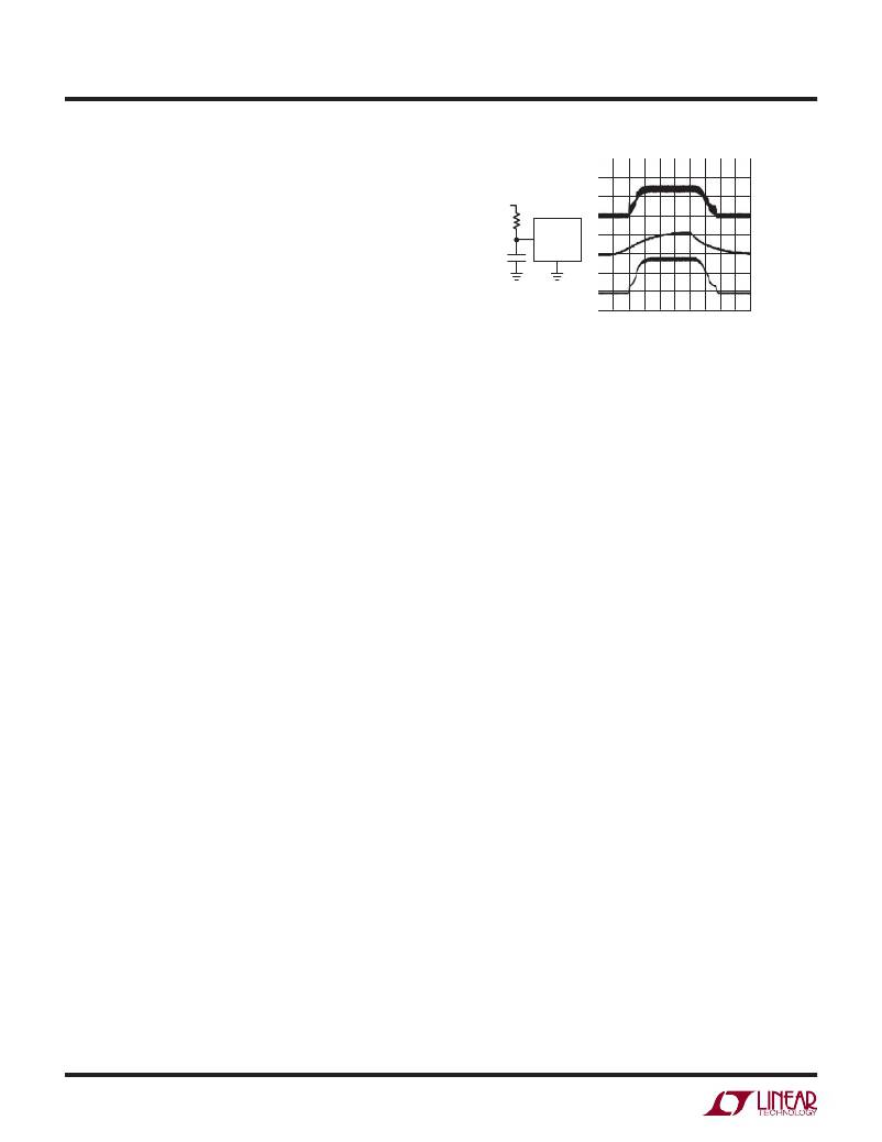
�Soft-Start�
�The� RUN/SS� pin� can� be� used� to� soft-start� the� LT1913,�
�reducing� the� maximum� input� current� during� start-up.�
�The� RUN/SS� pin� is� driven� through� an� external� RC� ?lter� to�
�create� a� voltage� ramp� at� this� pin.� Figure� 6� shows� the� start-�
�up� and� shut-down� waveforms� with� the� soft-start� circuit.�
�By� choosing� a� large� RC� time� constant,� the� peak� start-up�
�current� can� be� reduced� to� the� current� that� is� required� to�
�regulate� the� output,� with� no� overshoot.� Choose� the� value�
�of� the� resistor� so� that� it� can� supply� 20μA� when� the� RUN/SS�
�pin� reaches� 2.5V.�
�Synchronization�
�Synchronizing� the� LT1913� oscillator� to� an� external� fre-�
�quency� can� be� done� by� connecting� a� square� wave� (with�
�20%� to� 80%� duty� cycle)� to� the� SYNC� pin.� The� square�
�wave� amplitude� should� have� valleys� that� are� below� 0.3V�
�and� peaks� that� are� above� 0.8V� (up� to� 6V).�
�The� LT1913� may� be� synchronized� over� a� 250kHz� to� 2MHz�
�range.� The� R� T� resistor� should� be� chosen� to� set� the� LT1913�
�switching� frequency� 20%� below� the� lowest� synchronization�
�Figure� 6.� To� Soft-Start� the� LT1913,� Add� a� Resisitor�
�and� Capacitor� to� the� RUN/SS� Pin�
�input.� For� example,� if� the� synchronization� signal� will� be�
�250kHz� and� higher,� the� R� T� should� be� chosen� for� 200kHz.�
�To� assure� reliable� and� safe� operation� the� LT1913� will� only�
�synchronize� when� the� output� voltage� is� near� regulation�
�as� indicated� by� the� PG� ?ag.� It� is� therefore� necessary� to�
�choose� a� large� enough� inductor� value� to� supply� the� required�
�output� current� at� the� frequency� set� by� the� R� T� resistor.� See�
�Inductor� Selection� section.� It� is� also� important� to� note� that�
�slope� compensation� is� set� by� the� R� T� value:� When� the� sync�
�frequency� is� much� higher� than� the� one� set� by� R� T� ,� the� slope�
�compensation� will� be� signi?cantly� reduced� which� may�
�require� a� larger� inductor� value� to� prevent� subharmonic�
�oscillation.�
�Shorted� and� Reversed� Input� Protection�
�If� the� inductor� is� chosen� so� that� it� won’t� saturate� exces-�
�sively,� an� LT1913� buck� regulator� will� tolerate� a� shorted�
�output.� There� is� another� situation� to� consider� in� systems�
�where� the� output� will� be� held� high� when� the� input� to� the�
�LT1913� is� absent.� This� may� occur� in� battery� charging� ap-�
�plications� or� in� battery� backup� systems� where� a� battery�
�or� some� other� supply� is� diode� OR-ed� with� the� LT1913’s�
�output.� If� the� V� IN� pin� is� allowed� to� ?oat� and� the� RUN/SS�
�pin� is� held� high� (either� by� a� logic� signal� or� because� it� is�
�tied� to� V� IN� ),� then� the� LT1913’s� internal� circuitry� will� pull�
�its� quiescent� current� through� its� SW� pin.� This� is� ?ne� if�
�your� system� can� tolerate� a� few� mA� in� this� state.� If� you�
�ground� the� RUN/SS� pin,� the� SW� pin� current� will� drop� to�
�essentially� zero.� However,� if� the� V� IN� pin� is� grounded� while�
�1913f�
�16�
�相关PDF资料 |
PDF描述 |
|---|---|
| LT1930AES5#TRM | IC REG BOOST ADJ 1A TSOT23-5 |
| LT1931AIS5#TRPBF | IC REG INV 1A TSOT23-5 |
| LT1933HS6#TRMPBF | IC REG BUCK ADJ 0.6A TSOT23-6 |
| LT1934IDCB-1#TRPBF | IC REG BUCK ADJ 60MA 6DFN |
| LT1935ES5#TRM | IC REG BST FLYBK SEPIC TSOT23-5 |
相关代理商/技术参数 |
参数描述 |
|---|---|
| LT1920 | 制造商:LINER 制造商全称:Linear Technology 功能描述:Single Resistor Gain Programmable, Precision Instrumentation Amplifier |
| LT1920C | 制造商:LINER 制造商全称:Linear Technology 功能描述:Single Resistor Gain Programmable, Precision Instrumentation Amplifier |
| LT1920CN8 | 功能描述:IC PREC INSTRUMENTATION AMP 8DIP RoHS:否 类别:集成电路 (IC) >> Linear - Amplifiers - Instrumentation 系列:- 标准包装:2,500 系列:- 放大器类型:通用 电路数:2 输出类型:满摆幅 转换速率:350 V/µs 增益带宽积:180MHz -3db带宽:320MHz 电流 - 输入偏压:12.5µA 电压 - 输入偏移:800µV 电流 - 电源:15mA 电流 - 输出 / 通道:85mA 电压 - 电源,单路/双路(±):2.5 V ~ 12.6 V,±1.25 V ~ 6.3 V 工作温度:-40°C ~ 85°C 安装类型:表面贴装 封装/外壳:8-TSSOP,8-MSOP(0.118",3.00mm 宽) 供应商设备封装:8-MSOP 包装:带卷 (TR) |
| LT1920CN8#PBF | 功能描述:IC PREC INSTRUMENTATION AMP 8DIP RoHS:是 类别:集成电路 (IC) >> Linear - Amplifiers - Instrumentation 系列:- 标准包装:2,500 系列:- 放大器类型:通用 电路数:2 输出类型:满摆幅 转换速率:350 V/µs 增益带宽积:180MHz -3db带宽:320MHz 电流 - 输入偏压:12.5µA 电压 - 输入偏移:800µV 电流 - 电源:15mA 电流 - 输出 / 通道:85mA 电压 - 电源,单路/双路(±):2.5 V ~ 12.6 V,±1.25 V ~ 6.3 V 工作温度:-40°C ~ 85°C 安装类型:表面贴装 封装/外壳:8-TSSOP,8-MSOP(0.118",3.00mm 宽) 供应商设备封装:8-MSOP 包装:带卷 (TR) |
| LT1920CS8 | 功能描述:IC PREC INSTRUMNTATION AMP 8SOIC RoHS:否 类别:集成电路 (IC) >> Linear - Amplifiers - Instrumentation 系列:- 标准包装:2,500 系列:- 放大器类型:通用 电路数:2 输出类型:满摆幅 转换速率:350 V/µs 增益带宽积:180MHz -3db带宽:320MHz 电流 - 输入偏压:12.5µA 电压 - 输入偏移:800µV 电流 - 电源:15mA 电流 - 输出 / 通道:85mA 电压 - 电源,单路/双路(±):2.5 V ~ 12.6 V,±1.25 V ~ 6.3 V 工作温度:-40°C ~ 85°C 安装类型:表面贴装 封装/外壳:8-TSSOP,8-MSOP(0.118",3.00mm 宽) 供应商设备封装:8-MSOP 包装:带卷 (TR) |
发布紧急采购,3分钟左右您将得到回复。