- 您现在的位置:买卖IC网 > PDF目录30766 > LT1952MPGN#PBF (LINEAR TECHNOLOGY CORP) SWITCHING CONTROLLER, 560 kHz SWITCHING FREQ-MAX, PDSO16 PDF资料下载
参数资料
| 型号: | LT1952MPGN#PBF |
| 厂商: | LINEAR TECHNOLOGY CORP |
| 元件分类: | 稳压器 |
| 英文描述: | SWITCHING CONTROLLER, 560 kHz SWITCHING FREQ-MAX, PDSO16 |
| 封装: | 0.150 INCH, LEAD FREE, PLASTIC, SSOP-16 |
| 文件页数: | 8/28页 |
| 文件大小: | 357K |
| 代理商: | LT1952MPGN#PBF |
第1页第2页第3页第4页第5页第6页第7页当前第8页第9页第10页第11页第12页第13页第14页第15页第16页第17页第18页第19页第20页第21页第22页第23页第24页第25页第26页第27页第28页
LT1952/LT1952-1
16
19521fe
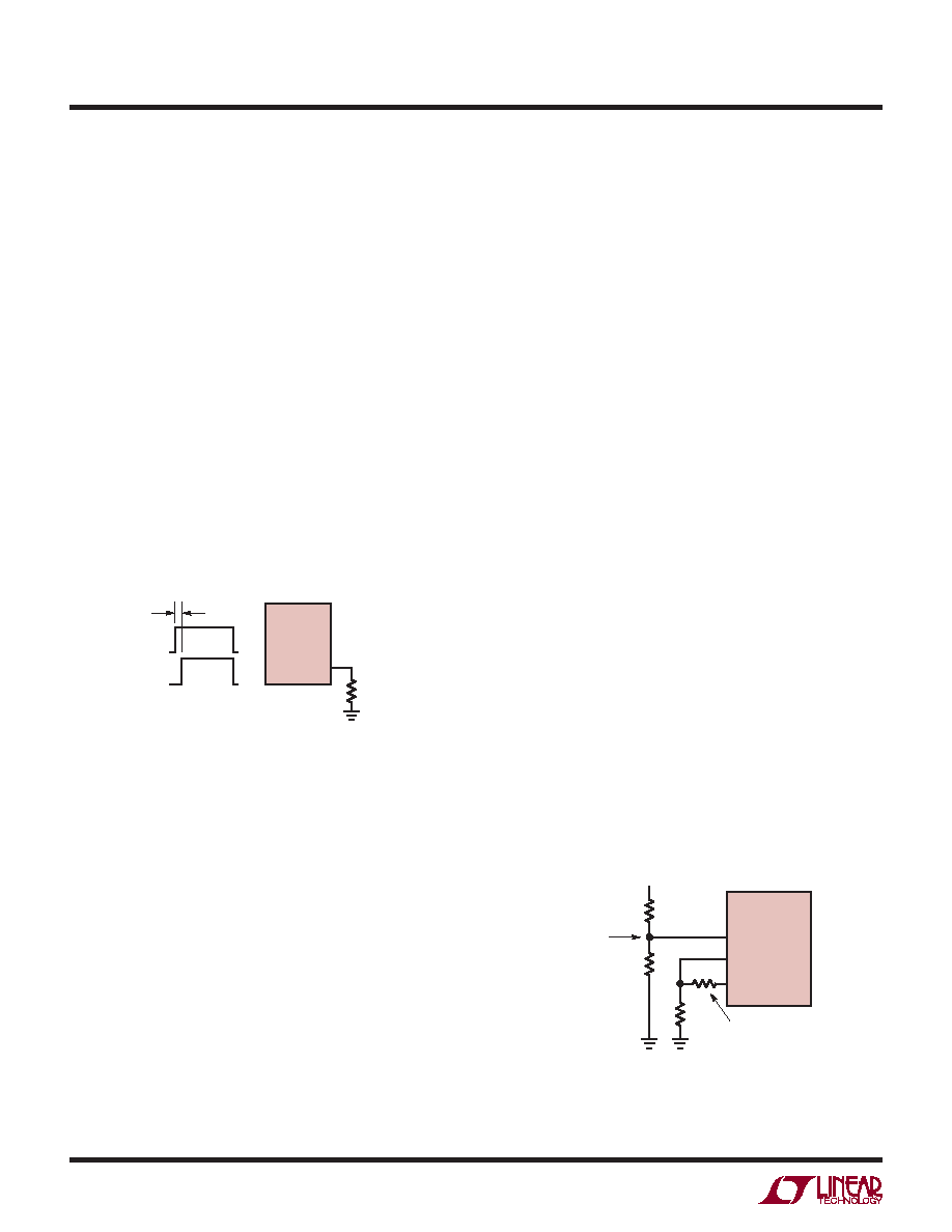
Programming Synchronous Rectifier Timing:
SOUT to OUT delay (‘tDELAY’)
The LT1952/LT1952-1 have an additional output SOUT
which provides a
±50mA peak drive clamped to 12V. In
applications requiring synchronous rectification for high
efficiency, the LT1952/LT1952-1 SOUT provides a sync
signal for secondary side control of the synchronous
rectifier MOSFETs (Figure 11). Timing delays through the
converter can cause non-optimum control timing for the
synchronous rectifier MOSFETs. The LT1952/LT1952-1
provide a programmable delay (tDELAY, Figure 8) between
SOUT rising edge and OUT rising edge to optimize timing
control for the synchronous rectifier MOSFETs to achieve
maximum efficiency gains. A resistor RDELAY connected
from the DELAY pin to ground sets the value of tDELAY.
Typical values for tDELAY range from 10ns with RDELAY =
10k to 160ns with RDELAY = 160k. (see graph in Typical
Performance Characteristics)
APPLICATIONS INFORMATION
SS_MAXDC pin using a resistor divider from VREF. An
increase of voltage at the SS_MAXDC pin causes the
maximum duty cycle clamp to increase.
To program the volt-second clamp, the following steps
should be taken:
(1)The maximum operational duty cycle of the converter
should be calculated for the given application.
(2)An initial value for the maximum duty cycle clamp
should be calculated using the equation below with a
first pass guess for SS_MAXDC.
Note: Since maximum operational duty cycle occurs at
minimum system input voltage (UVLO), the voltage at the
SD_VSEC pin = 1.32V.
Max Duty Cycle Clamp (OUT pin)
=k0.522(SS_MAXDC(DC)/SD_VSEC) –
(tDELAYfOSC)
where,
SS_MAXDC(DC) = VREF(RB/(RT + RB)
SD_VSEC = 1.32V at minimum system input voltage
tDELAY = programmed delay between SOUT and OUT
k = 1.11 – 5.5e–7(fOSC)
(3)Themaximumdutycycleclampcalculatedin(2)should
be programmed to be 10% greater than the maximum
operational duty cycle calculated in (1). Simple adjust-
ment of maximum duty cycle can be achieved by adjusting
SS_MAXDC.
Figure 8. Programming SOUT to OUT Delay: tDELAY
1952 F08
DELAY
LT1952/
LT1952-1
RDELAY
tDELAY
SOUT
OUT
Programming Maximum Duty Cycle Clamp
For forward converter applications using the simplest
topology of a single MOSFET on the primary, a maximum
switch duty cycle clamp which adapts to transformer
input voltage is necessary for reliable control of the
MOSFET. This volt-second clamp provides a safeguard for
transformerresetthatpreventstransformersaturation.The
LT1952/LT1952-1SD_VSECandSS_MAXDCpinsprovidea
capacitor-less,programmablevolt-secondclampsolution
using simple resistor ratios (Figure 9).
An increase of voltage at the SD_VSEC pin causes the
maximumdutycycleclamptodecrease.DerivingSD_VSEC
from a resistor divider connected to system input voltage
creates the volt-second clamp. The maximum duty cycle
clamp can be adjusted by programming voltage on the
Figure 9. Programming Maximum Duty Cycle Clamp
SYSTEM
INPUT VOLTAGE
ADAPTIVE
DUTY CYCLE
CLAMP INPUT
MAX DUTY CYCLE
CLAMP ADJUST INPUT
*MINIMUM ALLOWABLE RT IS 10k TO
GUARANTEE SOFT-START PULL-OFF
1952 F09
SD_VSEC
SS_MAXDC
VREF
LT1952/
LT1952-1
R1
R2
RB
RT*
相关PDF资料 |
PDF描述 |
|---|---|
| LT1952MPGN-1#TRPBF | SWITCHING CONTROLLER, 560 kHz SWITCHING FREQ-MAX, PDSO16 |
| LT1952MPGN#TRPBF | SWITCHING CONTROLLER, 560 kHz SWITCHING FREQ-MAX, PDSO16 |
| LT3412AIFE | 3 A SWITCHING REGULATOR, 4 kHz SWITCHING FREQ-MAX, PDSO16 |
| LT3412AEFE#TRPBF | 3 A SWITCHING REGULATOR, 4 kHz SWITCHING FREQ-MAX, PDSO16 |
| LT3412AEUF#TRPBF | 3 A SWITCHING REGULATOR, 4 kHz SWITCHING FREQ-MAX, PQCC16 |
相关代理商/技术参数 |
参数描述 |
|---|---|
| LT1956 | 制造商:LINEAR 制造商全称:LINEAR 功能描述:100V Synchronous Switching Regulator Controller |
| LT1956-5 | 制造商:LINER 制造商全称:Linear Technology 功能描述:High Voltage, 1.5A, 500kHz Step-Down Switching Regulators |
| LT1956EFE | 功能描述:IC REG BUCK ADJ 1.5A 16TSSOP RoHS:否 类别:集成电路 (IC) >> PMIC - 稳压器 - DC DC 开关稳压器 系列:- 设计资源:Design Support Tool 标准包装:1 系列:- 类型:升压(升压) 输出类型:固定 输出数:1 输出电压:3V 输入电压:0.75 V ~ 2 V PWM 型:- 频率 - 开关:- 电流 - 输出:100mA 同步整流器:是 工作温度:-40°C ~ 85°C 安装类型:表面贴装 封装/外壳:SOT-23-5 细型,TSOT-23-5 包装:剪切带 (CT) 供应商设备封装:TSOT-23-5 其它名称:AS1323-BTTT-30CT |
| LT1956EFE#PBF | 功能描述:IC REG BUCK ADJ 1.5A 16TSSOP RoHS:是 类别:集成电路 (IC) >> PMIC - 稳压器 - DC DC 开关稳压器 系列:- 标准包装:250 系列:- 类型:降压(降压) 输出类型:固定 输出数:1 输出电压:1.2V 输入电压:2.05 V ~ 6 V PWM 型:电压模式 频率 - 开关:2MHz 电流 - 输出:500mA 同步整流器:是 工作温度:-40°C ~ 85°C 安装类型:表面贴装 封装/外壳:6-UFDFN 包装:带卷 (TR) 供应商设备封装:6-SON(1.45x1) 产品目录页面:1032 (CN2011-ZH PDF) 其它名称:296-25628-2 |
| LT1956EFE#TR | 功能描述:IC REG BUCK ADJ 1.5A 16TSSOP RoHS:否 类别:集成电路 (IC) >> PMIC - 稳压器 - DC DC 开关稳压器 系列:- 设计资源:Design Support Tool 标准包装:1 系列:- 类型:升压(升压) 输出类型:固定 输出数:1 输出电压:3V 输入电压:0.75 V ~ 2 V PWM 型:- 频率 - 开关:- 电流 - 输出:100mA 同步整流器:是 工作温度:-40°C ~ 85°C 安装类型:表面贴装 封装/外壳:SOT-23-5 细型,TSOT-23-5 包装:剪切带 (CT) 供应商设备封装:TSOT-23-5 其它名称:AS1323-BTTT-30CT |
发布紧急采购,3分钟左右您将得到回复。