参数资料
| 型号: | LT3032IDE#PBF |
| 厂商: | Linear Technology |
| 文件页数: | 16/24页 |
| 文件大小: | 0K |
| 描述: | IC REG LDO ADJ .15A 14DFN |
| 产品培训模块: | LT3032 - 150mA Dual Positive/Negative Low Noise LDO |
| 特色产品: | LT3032 Voltage Linear Regulator |
| 标准包装: | 91 |
| 稳压器拓扑结构: | 正可调式和负可调式 |
| 输出电压: | ±1.22 V ~ ±20 V |
| 输入电压: | ±2.3 V ~ ±20 V |
| 电压 - 压降(标准): | 0.27V @ 150mA,0.3V @ -150mA |
| 稳压器数量: | 2 |
| 电流 - 输出: | 150mA |
| 电流 - 限制(最小): | 170mA |
| 工作温度: | -40°C ~ 125°C |
| 安装类型: | 表面贴装 |
| 封装/外壳: | 14-WFDFN 裸露焊盘 |
| 供应商设备封装: | 14-DFN(4x3) |
| 包装: | 管件 |
| 产品目录页面: | 1330 (CN2011-ZH PDF) |
�� �
�
�LT3032� Series�
�APPLICATIONS� INFORMATION�
�V� OUTP� =� 1.22� V� ?� 1� +�
�?� +� (� I� ADJP� )� (� R� 2P� )�
�TheLT3032isadual150mApositiveandnegativelownoise�
�low� dropout� linear� regulator� with� micropower� quiescent�
�current� and� shutdown.� It� supplies� ±150mA� at� a� dropout�
�OUTP�
�LT3032�
�R2P�
�+�
�V� OUTP�
�V� ADJP� =� 1.22� V�
�?�
�?�
�R� 2P� ?�
�R� 1P� ?�
�of� 300mV.� Output� voltage� noise� can� be� lowered� on� the�
�positive� side� to� 20μV� RMS� and� to� 30μV� RMS� on� the� negative�
�ADJP�
�R1P�
�I� ADJP� =� 30� nA� at� 25� °� C�
�OUTPUT� RANGE� =� 1.22� V� TO� 20� V�
�V� OUTN� =� –1.22� V� ?� 1� +�
�?� +� (� I� ADJN� )� (� R� 2N� )�
�sideoverthe10Hzto100kHzbandwidthwiththeaddition�
�of� 0.01μF� reference� bypass� capacitors.� Additionally,� the�
�GND�
�R1N�
�?�
�?�
�R� 2N� ?�
�R� 1N� ?�
�reference� bypass� capacitors� improve� transient� response,�
�lowering� the� settling� time� for� transient� load� conditions.�
�Quiescent� current� is� 25μA� for� the� positive� side� and� –30μA�
�ADJN�
�OUTN�
�R2N�
�+�
�V� OUTN�
�V� ADJN� =� –1.22� V�
�I� ADJN� =� –30� nA� at� 25� °� C�
�OUTPUT� RANGE� =� –1.22� V� TO� –� 20� V�
�for� the� negative� side� (45μA� each� for� the� LT3032-12/�
�LT3032-15),� typically� dropping� to� less� than� 3μA� total� in�
�shutdown.� In� addition� to� the� low� quiescent� current,� the�
�LT3032� incorporates� several� protection� features� which�
�make� it� ideal� for� use� in� battery-powered� systems.� If� the�
�load� is� common� mode� between� the� two� outputs,� it� does�
�not� matter� which� output� starts� ?rst;� either� output� can� be�
�pulled� to� the� opposing� side� of� ground� and� the� regulator�
�will� still� start� and� operate.�
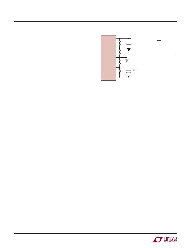
�Setting� Output� Voltage�
�The� adjustable� LT3032� has� output� voltage� ranges� of� 1.22V�
�to� 20V� for� the� positive� side� and� –1.22V� to� –20V� for� the�
�negative� side.� The� output� voltages� are� set� by� the� ratio� of�
�two� external� resistor� dividers� as� shown� in� Figure� 1.� The�
�LT3032� servos� the� outputs� to� maintain� the� voltages� at� the�
�ADJP� and� ADJN� pins� to� 1.22V� and� –1.22V,� respectively.�
�The� current� in� the� bottom� resistor� of� each� divider� (R1P�
�or� R1N)� is� equal� to� 1.22V/R1� and� the� current� in� the� top�
�resistor� (R2P� or� R2N)� is� equal� to� the� current� in� the� bottom�
�resistor� plus� the� respective� ADJP/ADJN� pin� bias� current.�
�The� bias� current� for� ADJP� and� ADJN� is� 30nA� at� 25°C,�
�?owing� into� the� pin� for� ADJP� and� ?owing� out� of� the� pin�
�for� ADJN.� The� output� voltages� can� then� be� calculated� us-�
�ing� the� formulas� shown� in� Figure� 1.� The� value� of� R1P� or�
�R1N� should� be� less� than� 250k� to� minimize� errors� in� the�
�resultant� output� voltage� caused� by� the� ADJP/ADJN� pin�
�bias� current.� Note� that� in� shutdown� the� respective� output�
�is� turned� off� and� the� divider� current� will� be� zero.� Curves�
�of� ADJP� Pin� Voltage,� ADJN� Pin� Voltage,� ADJP� Pin� Bias�
�Current,� and� ADJN� Pin� Bias� Current� (all� vs� Temperature)�
�3032� F01�
�Figure� 1.� Setting� Output� Voltages�
�The� LT3032� is� tested� and� speci?ed� with� the� ADJP/ADJN�
�pin� tied� to� the� respective� OUTP/OUTN� pin� and� a� ±5μA� DC�
�load� (unless� otherwise� speci?ed)� for� an� output� voltage�
�of� ±1.22V.� Speci?cations� for� output� voltages� greater� than�
�this� will� be� proportional� to� ±1.22V;� (V� OUT� /±1.22V).� For�
�example,� load� regulation� for� an� output� current� change�
�of� 1mA� to� 150mA� is� –2mV� typical� at� V� OUTN� =� –1.22V.� At�
�V� OUTN� =� –12V,� load� regulation� is:�
�(–12V/–1.22V)?(–2mV)� =� –19.6mV�
�Bypass� Capacitors� and� Low� Noise� Performance�
�The� LT3032� provides� reasonable� noise� performance�
�without� reference� bypass� capacitors� from� OUTP/OUTN�
�to� the� corresponding� BYPP/BYPN� pin.� Using� the� LT3032�
�with� the� addition� of� reference� bypass� capacitors� lowers�
�output� voltage� noise.� Good� quality� low� leakage� capacitors�
�are� recommended.� These� capacitors� bypass� the� internal�
�references� for� the� positive� and� negative� sides� of� the� LT3032,�
�providing� low� frequency� noise� poles.� The� noise� poles�
�provided� by� the� bypass� capacitors� decrease� the� output�
�voltage� noise� to� as� low� as� 20μV� RMS� for� the� positive� side�
�and� 30μV� RMS� for� the� negative� side� with� the� use� of� 0.01μF�
�bypass� capacitors.�
�The� BYPP� pin� and� BYPN� pin� are� high� impedance� nodes�
�and� leakage� into� or� out� of� these� pins� affects� the� reference�
�voltage.� The� BYPP� pin� operates� at� approximately� 74mV� at�
�appear� in� the� Typical� Performance� Characteristics.�
�3032fd�
�16�
�相关PDF资料 |
PDF描述 |
|---|---|
| RSM36DTBD-S664 | CONN EDGECARD 72POS R/A .156 |
| LFECP6E-3FN484I | IC FPGA 6.1KLUTS 484FPBGA |
| LFEC6E-3T144I | IC FPGA 6.1KLUTS 97I/O 144-TQFP |
| MAX4945LELA+T | IC CTLR OVP W/FET 5.80V 8UDFN |
| MAX4945AELA+T | IC CTLR OVP W/FET 5.80V 8UDFN |
相关代理商/技术参数 |
参数描述 |
|---|---|
| LT3032IDETR | 制造商:LINER 制造商全称:Linear Technology 功能描述:Dual 150mA Positive/Negative Low Noise Low Dropout Linear Regulator |
| LT3032IDETRPBF | 制造商:LINER 制造商全称:Linear Technology 功能描述:Dual 150mA Positive/Negative Low Noise Low Dropout Linear Regulator |
| LT3032MPDE#PBF | 功能描述:IC REG LDO ADJ .15A 14-DFN RoHS:是 类别:集成电路 (IC) >> PMIC - 稳压器 - 线性 系列:- 标准包装:3,000 系列:- 稳压器拓扑结构:正,固定式 输出电压:2.5V 输入电压:2.5 V ~ 5.5 V 电压 - 压降(标准):- 稳压器数量:1 电流 - 输出:300mA(最小值) 电流 - 限制(最小):360mA 工作温度:-40°C ~ 85°C 安装类型:表面贴装 封装/外壳:SOT-23-5 细型,TSOT-23-5 供应商设备封装:TSOT-23-5 包装:带卷 (TR) |
| LT3032MPDE#TRPBF | 功能描述:IC REG LDO ADJ .15A 14-DFN RoHS:是 类别:集成电路 (IC) >> PMIC - 稳压器 - 线性 系列:- 标准包装:3,000 系列:- 稳压器拓扑结构:正,固定式 输出电压:2.5V 输入电压:2.5 V ~ 5.5 V 电压 - 压降(标准):- 稳压器数量:1 电流 - 输出:300mA(最小值) 电流 - 限制(最小):360mA 工作温度:-40°C ~ 85°C 安装类型:表面贴装 封装/外壳:SOT-23-5 细型,TSOT-23-5 供应商设备封装:TSOT-23-5 包装:带卷 (TR) |
| LT3032MPDE-12#PBF | 功能描述:IC REG LDO +-12V .15A 14-DFN RoHS:是 类别:集成电路 (IC) >> PMIC - 稳压器 - 线性 系列:- 标准包装:3,000 系列:- 稳压器拓扑结构:正,固定式 输出电压:2.5V 输入电压:2.5 V ~ 5.5 V 电压 - 压降(标准):- 稳压器数量:1 电流 - 输出:300mA(最小值) 电流 - 限制(最小):360mA 工作温度:-40°C ~ 85°C 安装类型:表面贴装 封装/外壳:SOT-23-5 细型,TSOT-23-5 供应商设备封装:TSOT-23-5 包装:带卷 (TR) |
发布紧急采购,3分钟左右您将得到回复。