参数资料
| 型号: | LT3070EUFD#TRPBF |
| 厂商: | Linear Technology |
| 文件页数: | 16/28页 |
| 文件大小: | 0K |
| 描述: | IC REG LDO ADJ 5A 28QFN |
| 产品培训模块: | LT3070 - 5A, Low Noise, Programmable Output, 85mV Dropout Linear Regulator |
| 标准包装: | 2,500 |
| 稳压器拓扑结构: | 正,可调式 |
| 输出电压: | 0.8 V ~ 1.8 V |
| 输入电压: | 0.95 V ~ 3 V |
| 电压 - 压降(标准): | 0.085V @ 5A |
| 稳压器数量: | 1 |
| 电流 - 输出: | 5A |
| 电流 - 限制(最小): | 5.1A |
| 工作温度: | -40°C ~ 125°C |
| 安装类型: | 表面贴装 |
| 封装/外壳: | 28-WFQFN 裸露焊盘 |
| 供应商设备封装: | 28-QFN(4x5) |
| 包装: | 带卷 (TR) |
第1页第2页第3页第4页第5页第6页第7页第8页第9页第10页第11页第12页第13页第14页第15页当前第16页第17页第18页第19页第20页第21页第22页第23页第24页第25页第26页第27页第28页
�� �
�
�LT3070�
�APPLICATIONS� INFORMATION�
�component� cost� savings.� The� LT3070� steps� to� the� next�
�level� of� performance� for� the� latest� generation� FPGAs,� DSPs�
�and� microprocessors.� The� simple� versatility� and� benefits�
�derived� from� these� circuits� exceed� the� power� supply� needs�
�of� today’s� high� performance� microprocessors.�
�Programming� Output� Voltage�
�Three� tri-level� input� pins,� V� O2� ,� V� O1� and� V� O0� ,� select� the�
�value� of� output� voltage.� Table� 1� illustrates� the� 3-bit� digital�
�word� to� output� voltage� resulting� from� setting� these� pins�
�high� ,� low� or� allowing� them� to� float.�
�These� pins� may� be� tied� high� or� low� by� either� pin-strapping�
�them� to� V� BIAS� or� driving� them� with� digital� ports.� Pins� that�
�float� may� either� actually� float� or� require� logic� that� has�
�Hi-Z� output� capability.� This� allows� output� voltage� to� be�
�dynamically� changed� if� necessary.�
�Output� voltage� is� selectable� from� a� minimum� of� 0.8V� to�
�a� maximum� of� 1.8V� in� increments� of� 50mV.� The� MSB,�
�V� O2� ,� sets� the� pedestal� voltage,� and� the� LSB’s,� V� O1� and�
�V� O0� increment� V� OUT� .�
�Output� voltage� is� limited� to� 1.8V� maximum� by� an� internal�
�override� of� V� O1� (default� to� low� )� when� V� O2� =� high� .�
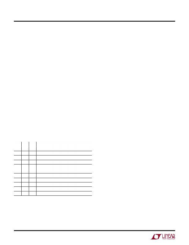
�Table� 1: V� O2� to V� O0� Settings� vs� Output� V� oltag� e�
�V� O2� V� O1� V� O0� V� OUT(NOM)� V� O2� V� O1� V� O0� V� OUT(NOM)�
�0� 0� 0� 0.80V� Z� 0� 1� 1.35V�
�0� 0� Z� 0.85V� Z� Z� 0� 1.40V�
�0� 0� 1� 0.90V� Z� Z� Z� 1.45V�
�0� Z� 0� 0.95V� Z� Z� 1� 1.50V�
�0� Z� Z� 1.00V� Z� 1� 0� 1.55V�
�0� Z� 1� 1.05V� Z� 1� Z� 1.60V�
�0� 1� 0� 1.10V� Z� 1� 1� 1.65V�
�0� 1� Z� 1.15V� 1� X� 0� 1.70V�
�0� 1� 1� 1.20V� 1� X� Z� 1.75V�
�Z� 0� 0� 1.25V� 1� X� 1� 1.80V�
�Z� 0� Z� 1.30V�
�X� =� Don’t� Care,� 0� =� Low,� Z� =� Float,� 1� =� High�
�The� input� logic� low� threshold� is� less� than� 250mV� refer-�
�enced� to� GND� and� the� logic� high� threshold� is� greater� than�
�V� BIAS� –� 250mV.� The� range� between� these� two� thresholds�
�as� set� by� a� window� comparator� defines� the� logic� Hi-Z�
�state.�
�REF/BYP—Voltage� Reference�
�This� pin� is� the� buffered� output� of� the� internal� bandgap�
�reference� and� has� an� output� impedance� of� ?� 19kΩ.� The�
�design� includes� an� internal� compensation� pole� at� f� C� =�
�4kHz.� A� 10nF� REF/BYP� capacitor� to� GND� creates� a� low-�
�pass� pole� at� f� LP� =� 840Hz.� The� 10nF� capacitor� decreases�
�reference� voltage� noise� to� about� 10μV� RMS� and� soft-starts�
�the� reference.� The� LT3070� only� soft-starts� the� reference�
�voltage� during� an� initial� turn-on� sequence.� If� the� EN� pin�
�is� toggled� low� after� initial� turn-on,� the� reference� remains�
�powered-up.� Therefore,� toggling� the� EN� pin� from� low� to�
�high� does� not� soft-start� the� reference.� Only� by� turning�
�the� BIAS� supply� voltage� on� and� off� will� the� reference� be�
�soft-started.� Output� voltage� noise� is� the� RMS� sum� of� the�
�reference� voltage� noise� in� addition� to� the� amplifier� noise.�
�The� REF/BYP� pin� must� not� be� DC� loaded� by� anything� except�
�for� applications� that� parallel� other� LT3070� regulators� for�
�higher� output� currents.� Consult� the� Applications� Section�
�on� Paralleling� for� further� details.�
�Output� Voltage� Margining�
�Two� tri-level� input� pins,� MARGSEL� (polarity)� and� MARGTOL�
�(scale),� select� the� polarity� and� amount� of� output� voltage�
�margining.� Margining� is� programmable� in� increments� of�
�±1%,� ±3%� and� ±5%.� Margining� is� internally� implemented�
�as� a� scaling� of� the� reference� voltage.�
�Table� 2� illustrates� the� 2-bit� digital� word� to� output� voltage�
�margining� resulting� from� setting� these� pins� high,� low� or�
�allowing� them� to� float.�
�These� pins� may� be� set� high� or� low� by� either� pin-strapping�
�them� to� V� BIAS� or� driving� them� with� digital� ports.� Pins� that�
�float� may� either� actually� float� or� require� logic� that� has�
�“Hi-Z”� output� capability.� This� allows� output� voltage� to� be�
�dynamically� margined� if� necessary.�
�The� MARGSEL� pin� determines� both� the� polarity� and� the� ac-�
�tive� state� of� the� margining� function.� The� logic� low� threshold�
�is� less� than� 250mV� referenced� to� GND� and� enables� negative�
�voltage� margining.� The� logic� high� threshold� is� greater� than�
�V� BIAS� –� 250mV� and� enables� positive� voltage� margining.�
�The� voltage� range� between� these� two� logic� thresholds� as�
�set� by� a� window� comparator� defines� the� logic� Hi-Z� state�
�and� disables� the� margining� function.�
�3070fb�
�16�
�For� more� information� www.linear.com/LT3070�
�相关PDF资料 |
PDF描述 |
|---|---|
| MIC5310-SGYML TR | IC REG LDO 3.3V/1.8V .15A 8-MLF |
| GBB90DHBD | CONN EDGECARD 180PS R/A .050 SLD |
| HCC65DREI-S93 | CONN EDGECARD 130PS .100 EYELET |
| HBC65DREI-S93 | CONN EDGECARD 130PS .100 EYELET |
| EMC50DRTN-S93 | CONN EDGECARD 100PS DIP .100 SLD |
相关代理商/技术参数 |
参数描述 |
|---|---|
| LT3070IUFD | 制造商:LINER 制造商全称:Linear Technology 功能描述:5A, Low Noise, Programmable Output, 85mV Dropout Linear Regulator |
| LT3070IUFD#PBF | 功能描述:IC REG LDO ADJ 5A 28QFN RoHS:是 类别:集成电路 (IC) >> PMIC - 稳压器 - 线性 系列:- 标准包装:1 系列:- 稳压器拓扑结构:正,固定式 输出电压:8V 输入电压:10.5 V ~ 23 V 电压 - 压降(标准):1.7V @ 40mA 稳压器数量:1 电流 - 输出:100mA(最小值) 电流 - 限制(最小):- 工作温度:0°C ~ 125°C 安装类型:表面贴装 封装/外壳:8-SOIC(0.154",3.90mm 宽) 供应商设备封装:8-SOIC 包装:剪切带 (CT) 产品目录页面:1075 (CN2011-ZH PDF) 其它名称:296-24390-1 |
| LT3070IUFD#TRPBF | 功能描述:IC REG LDO ADJ 5A 28QFN RoHS:是 类别:集成电路 (IC) >> PMIC - 稳压器 - 线性 系列:- 标准包装:3,000 系列:- 稳压器拓扑结构:正,固定式 输出电压:2.5V 输入电压:2.5 V ~ 5.5 V 电压 - 压降(标准):- 稳压器数量:1 电流 - 输出:300mA(最小值) 电流 - 限制(最小):360mA 工作温度:-40°C ~ 85°C 安装类型:表面贴装 封装/外壳:SOT-23-5 细型,TSOT-23-5 供应商设备封装:TSOT-23-5 包装:带卷 (TR) |
| LT3070IUFDPBF | 制造商:LINER 制造商全称:Linear Technology 功能描述:5A, Low Noise, Programmable Output, 85mV Dropout Linear Regulator |
| LT3070IUFDTR | 制造商:LINER 制造商全称:Linear Technology 功能描述:5A, Low Noise, Programmable Output, 85mV Dropout Linear Regulator |
发布紧急采购,3分钟左右您将得到回复。