- 您现在的位置:买卖IC网 > PDF目录79982 > LT3579EFE-1#PBF (LINEAR TECHNOLOGY CORP) SWITCHING REGULATOR, PDSO20 PDF资料下载
参数资料
| 型号: | LT3579EFE-1#PBF |
| 厂商: | LINEAR TECHNOLOGY CORP |
| 元件分类: | 稳压器 |
| 英文描述: | SWITCHING REGULATOR, PDSO20 |
| 封装: | 4.40 MM, LEAD FREE, PLASTIC, TSSOP-20 |
| 文件页数: | 8/40页 |
| 文件大小: | 503K |
| 代理商: | LT3579EFE-1#PBF |
第1页第2页第3页第4页第5页第6页第7页当前第8页第9页第10页第11页第12页第13页第14页第15页第16页第17页第18页第19页第20页第21页第22页第23页第24页第25页第26页第27页第28页第29页第30页第31页第32页第33页第34页第35页第36页第37页第38页第39页第40页
LT3579/LT3579-1
16
35791f
applicaTions inForMaTion
LAYOUT GUIDELINES FOR BOOST, SEPIC, AND DUAL
INDUCTOR INVERTING TOPOLOGIES
General Layout Guidelines
To optimize thermal performance, solder the exposed
ground pad of the LT3579 to the ground plane with
multiple vias around the pad connecting to additional
ground planes.
Agroundplaneshouldbeusedundertheswitchercircuitry
to prevent interplane coupling and overall noise.
Highspeedswitchingpath(seespecifictopologybelowfor
more information) must be kept as short as possible.
The VC, FB, and RT components should be placed as
close to the LT3579 as possible, while being as far
away as practically possible from the switch node. The
groundforthesecomponentsshouldbeseparatedfrom
the switch current path.
Place the bypass capacitor for the VIN pin (CVIN) as
close as possible to the LT3579.
Place the bypass capacitor for the inductor (CPWR) as
close as possible to the inductor.
Bypass capacitors, CPWR and CVIN, may be combined
into a single bypass capacitor, CIN,iftheinputsideofthe
inductor can be close to the VIN pin of the LT3579.
The load should connect directly to the positive and
negative terminals of the output capacitor for best load
regulation.
Boost Topology Specific Layout Guidelines
Keep length of loop (high speed switching path)
governing switch, diode D1, output capacitor COUT,and
ground return as short as possible to minimize parasitic
inductive spikes at the switch node during switching.
SEPIC Topology Specific Layout Guidelines
Keeplengthofloop(highspeedswitchingpath)governing
switch,flyingcapacitorC1,diodeD1,outputcapacitorCOUT,
andgroundreturnasshortaspossibletominimizeparasitic
inductive spikes at the switch node during switching.
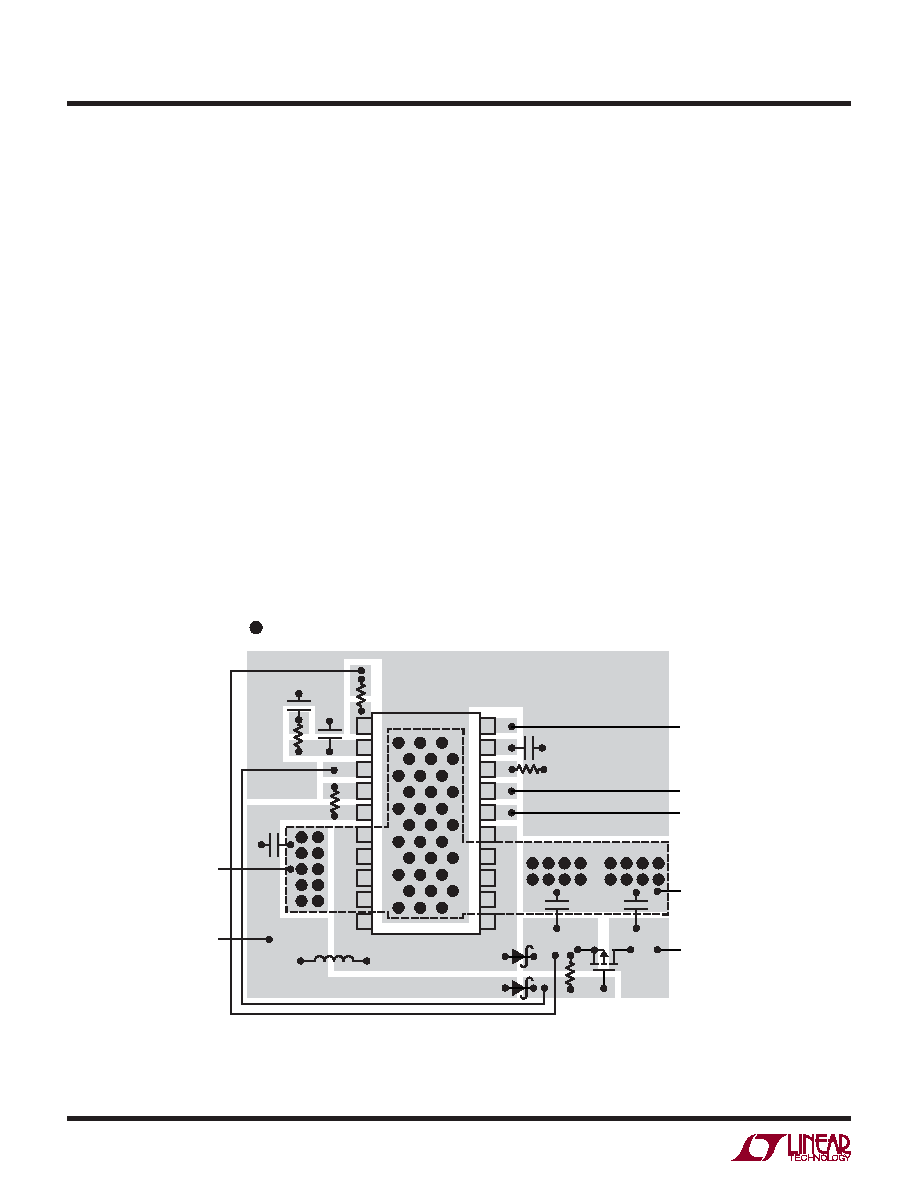
Figure 9. Suggested Component Placement for Boost Topology in FE20 Package
A– RETURN CIN GROUND DIRECTLY TO LT3579 EXPOSED PAD PIN 21. IT IS ADVISED TO NOT COMBINE CIN GROUND
WITH GND EXCEPT AT THE EXPOSED PAD.
B– RETURN COUT AND COUT1 GROUND DIRECTLY TO LT3579 EXPOSED PAD PIN 21. IT IS ADVISED TO NOT COMBINE
COUT AND COUT1 GROUND WITH GND EXCEPT AT THE EXPOSED PAD.
1
2
3
4
5
6
7
8
9
10
20
19
18
17
16
15
14
13
12
11
21
GND
CIN
VIN
RGATE
–
+
–
VOUT
COUT
COUT1
A
B
SYNC
CLKOUT
SHDN
VIAS TO GROUND PLANE REQUIRED TO IMPROVE
THERMAL PERFORMANCE
35791 F08
M1
D1
D2
L1
相关PDF资料 |
PDF描述 |
|---|---|
| LTC3521IFE#TRPBF | SWITCHING REGULATOR, 1350 kHz SWITCHING FREQ-MAX, PDSO20 |
| LS4501-9PD6TB1 | 1-OUTPUT 100 W AC-DC PWR FACTOR CORR MODULE |
| LK2320-7EPD2TB1 | 2-OUTPUT 150 W AC-DC REG PWR SUPPLY MODULE |
| LK2540-7EPD2TB1 | 2-OUTPUT 150 W AC-DC REG PWR SUPPLY MODULE |
| LS1001-7EPD7T | 1-OUTPUT 100 W AC-DC REG PWR SUPPLY MODULE |
相关代理商/技术参数 |
参数描述 |
|---|---|
| LT3579EFE-1-TRPBF | 制造商:LINER 制造商全称:Linear Technology 功能描述:6A Boost/Inverting DC/DC Converter with Fault Protection |
| LT3579EFE-PBF | 制造商:LINER 制造商全称:Linear Technology 功能描述:6A Boost/Inverting DC/DC Converter with Fault Protection |
| LT3579EFE-TRPBF | 制造商:LINER 制造商全称:Linear Technology 功能描述:6A Boost/Inverting DC/DC Converter with Fault Protection |
| LT3579EUFD#PBF | 功能描述:IC REG MULTI CONFIG SYNC 20QFN RoHS:是 类别:集成电路 (IC) >> PMIC - 稳压器 - DC DC 开关稳压器 系列:- 标准包装:2,500 系列:- 类型:降压(降压) 输出类型:固定 输出数:1 输出电压:1.2V,1.5V,1.8V,2.5V 输入电压:2.7 V ~ 20 V PWM 型:- 频率 - 开关:- 电流 - 输出:50mA 同步整流器:是 工作温度:-40°C ~ 125°C 安装类型:表面贴装 封装/外壳:10-TFSOP,10-MSOP(0.118",3.00mm 宽)裸露焊盘 包装:带卷 (TR) 供应商设备封装:10-MSOP 裸露焊盘 |
| LT3579EUFD#TRPBF | 功能描述:IC REG MULTI CONFIG SYNC 20QFN RoHS:是 类别:集成电路 (IC) >> PMIC - 稳压器 - DC DC 开关稳压器 系列:- 标准包装:2,500 系列:- 类型:降压(降压) 输出类型:固定 输出数:1 输出电压:1.2V,1.5V,1.8V,2.5V 输入电压:2.7 V ~ 20 V PWM 型:- 频率 - 开关:- 电流 - 输出:50mA 同步整流器:是 工作温度:-40°C ~ 125°C 安装类型:表面贴装 封装/外壳:10-TFSOP,10-MSOP(0.118",3.00mm 宽)裸露焊盘 包装:带卷 (TR) 供应商设备封装:10-MSOP 裸露焊盘 |
发布紧急采购,3分钟左右您将得到回复。