- 您现在的位置:买卖IC网 > PDF目录79982 > LT3579EFE-1#PBF (LINEAR TECHNOLOGY CORP) SWITCHING REGULATOR, PDSO20 PDF资料下载
参数资料
| 型号: | LT3579EFE-1#PBF |
| 厂商: | LINEAR TECHNOLOGY CORP |
| 元件分类: | 稳压器 |
| 英文描述: | SWITCHING REGULATOR, PDSO20 |
| 封装: | 4.40 MM, LEAD FREE, PLASTIC, TSSOP-20 |
| 文件页数: | 9/40页 |
| 文件大小: | 503K |
| 代理商: | LT3579EFE-1#PBF |
第1页第2页第3页第4页第5页第6页第7页第8页当前第9页第10页第11页第12页第13页第14页第15页第16页第17页第18页第19页第20页第21页第22页第23页第24页第25页第26页第27页第28页第29页第30页第31页第32页第33页第34页第35页第36页第37页第38页第39页第40页
LT3579/LT3579-1
17
35791f
the heat generated within the package. This can be
accomplished by taking advantage of the thermal pad on
the underside of the IC. It is recommended that multiple
vias in the printed circuit board be used to conduct heat
away from the IC and into a copper plane with as much
area as possible.
Power & Thermal Calculations
Power dissipation in the LT3579 chip comes from four
primary sources: switch I2R loss, NPN base drive loss
(AC), NPN base drive loss (DC), and additional VIN pin
current. These formulas assume continuous mode
operation, so they should not be used for calculating
thermal losses or efficiency in discontinuous mode or at
light load currents.
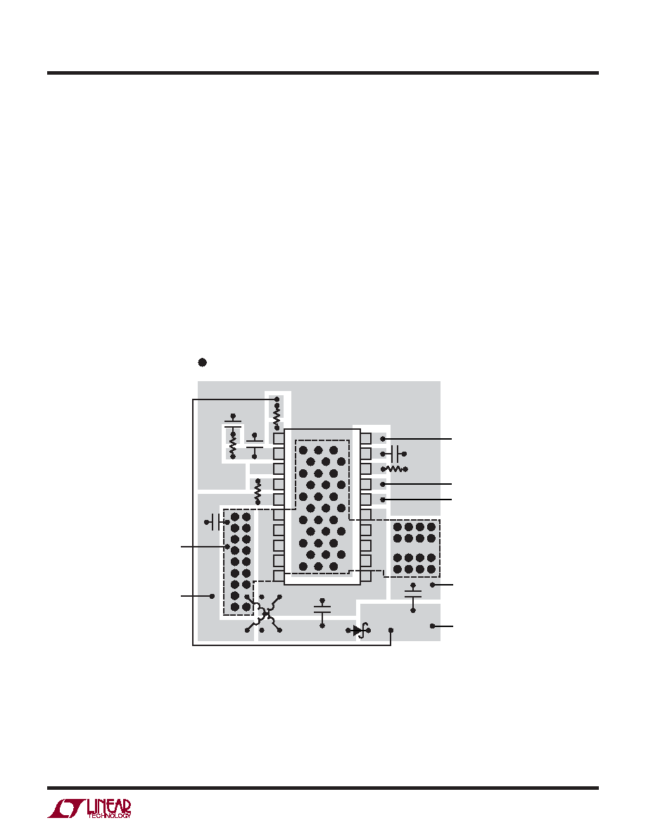
Inverting Topology Specific Layout Guidelines
Keep ground return path from the cathode of D1 (to
chip) separated from output capacitor COUT’s ground
return path (to chip) in order to minimize switching
noise coupling into the output. Notice the separate
ground return for D1’s cathode in Figure 11.
Keep length of loop (high speed switching path)
governing switch, flying capacitor C1, diode D1, and
ground return as short as possible to minimize parasitic
inductive spikes at the switch node during switching.
THERMAL CONSIDERATIONS
For the LT3579 to deliver its full output power, it is imp-
erative that a good thermal path be provided to dissipate
A– RETURN CIN AND L2 GROUND DIRECTLY TO LT3579 EXPOSED PAD PIN 21. IT IS ADVISED TO NOT COMBINE CIN AND L2 GROUND WITH GND EXCEPT AT THE EXPOSED PAD.
B– RETURN COUT GROUND DIRECTLY TO LT3579 EXPOSED PAD PIN 21. IT IS ADVISED TO NOT COMBINE COUT GROUND WITH GND EXCEPT AT THE EXPOSED PAD.
L1, L2 –MOST COUPLED INDUCTOR MANUFACTURERS USE CROSS PINOUT FOR IMPROVED PERFORMANCE.
1
2
3
4
5
6
7
8
9
10
20
19
18
17
16
15
14
13
12
11
21
GND
CIN
VIN
–
+
–
VOUT
COUT
A
B
SYNC
CLKOUT
SHDN
VIAS TO GROUND PLANE REQUIRED TO IMPROVE
THERMAL PERFORMANCE
35791 F10
L1
L2
D1
C1
Figure 10. Suggested Component Placement for SEPIC Topology in FE20 Package
applicaTions inForMaTion
相关PDF资料 |
PDF描述 |
|---|---|
| LTC3521IFE#TRPBF | SWITCHING REGULATOR, 1350 kHz SWITCHING FREQ-MAX, PDSO20 |
| LS4501-9PD6TB1 | 1-OUTPUT 100 W AC-DC PWR FACTOR CORR MODULE |
| LK2320-7EPD2TB1 | 2-OUTPUT 150 W AC-DC REG PWR SUPPLY MODULE |
| LK2540-7EPD2TB1 | 2-OUTPUT 150 W AC-DC REG PWR SUPPLY MODULE |
| LS1001-7EPD7T | 1-OUTPUT 100 W AC-DC REG PWR SUPPLY MODULE |
相关代理商/技术参数 |
参数描述 |
|---|---|
| LT3579EFE-1-TRPBF | 制造商:LINER 制造商全称:Linear Technology 功能描述:6A Boost/Inverting DC/DC Converter with Fault Protection |
| LT3579EFE-PBF | 制造商:LINER 制造商全称:Linear Technology 功能描述:6A Boost/Inverting DC/DC Converter with Fault Protection |
| LT3579EFE-TRPBF | 制造商:LINER 制造商全称:Linear Technology 功能描述:6A Boost/Inverting DC/DC Converter with Fault Protection |
| LT3579EUFD#PBF | 功能描述:IC REG MULTI CONFIG SYNC 20QFN RoHS:是 类别:集成电路 (IC) >> PMIC - 稳压器 - DC DC 开关稳压器 系列:- 标准包装:2,500 系列:- 类型:降压(降压) 输出类型:固定 输出数:1 输出电压:1.2V,1.5V,1.8V,2.5V 输入电压:2.7 V ~ 20 V PWM 型:- 频率 - 开关:- 电流 - 输出:50mA 同步整流器:是 工作温度:-40°C ~ 125°C 安装类型:表面贴装 封装/外壳:10-TFSOP,10-MSOP(0.118",3.00mm 宽)裸露焊盘 包装:带卷 (TR) 供应商设备封装:10-MSOP 裸露焊盘 |
| LT3579EUFD#TRPBF | 功能描述:IC REG MULTI CONFIG SYNC 20QFN RoHS:是 类别:集成电路 (IC) >> PMIC - 稳压器 - DC DC 开关稳压器 系列:- 标准包装:2,500 系列:- 类型:降压(降压) 输出类型:固定 输出数:1 输出电压:1.2V,1.5V,1.8V,2.5V 输入电压:2.7 V ~ 20 V PWM 型:- 频率 - 开关:- 电流 - 输出:50mA 同步整流器:是 工作温度:-40°C ~ 125°C 安装类型:表面贴装 封装/外壳:10-TFSOP,10-MSOP(0.118",3.00mm 宽)裸露焊盘 包装:带卷 (TR) 供应商设备封装:10-MSOP 裸露焊盘 |
发布紧急采购,3分钟左右您将得到回复。