- 您现在的位置:买卖IC网 > PDF目录1825 > LT3580MPMS8E#TRPBF (Linear Technology)IC REG BOOST INV SEPIC 2A 8MSOP PDF资料下载
参数资料
| 型号: | LT3580MPMS8E#TRPBF |
| 厂商: | Linear Technology |
| 文件页数: | 13/28页 |
| 文件大小: | 0K |
| 描述: | IC REG BOOST INV SEPIC 2A 8MSOP |
| 标准包装: | 2,500 |
| 类型: | 升压(升压),反相,Sepic |
| 输出数: | 1 |
| 输入电压: | 2.5 V ~ 32 V |
| PWM 型: | 电流模式 |
| 频率 - 开关: | 200kHz ~ 2.5MHz |
| 电流 - 输出: | 2A |
| 同步整流器: | 无 |
| 工作温度: | -55°C ~ 125°C |
| 安装类型: | 表面贴装 |
| 封装/外壳: | 8-TSSOP,8-MSOP(0.118",3.00mm 宽)裸露焊盘 |
| 包装: | 带卷 (TR) |
| 供应商设备封装: | 8-MSOP-EP |
第1页第2页第3页第4页第5页第6页第7页第8页第9页第10页第11页第12页当前第13页第14页第15页第16页第17页第18页第19页第20页第21页第22页第23页第24页第25页第26页第27页第28页
�� �
�
�LT3580�
�APPLICATIONS� INFORMATION�
�(1)� SYNC� may� not� toggle� outside� the� frequency� range� of�
�200kHz� to� 2.5MHz� unless� it� is� stopped� low� to� enable�
�the� free-running� oscillator.�
�(2)� The� SYNC� frequency� can� always� be� higher� than� the�
�free-running� oscillator� frequency,� f� OSC� ,� but� should� not�
�be� less� than� 25%� below� f� OSC� .�
�Operating� Frequency� Selection�
�There� are� several� considerations� in� selecting� the� operating�
�frequency� of� the� converter.� The� first� is� staying� clear� of�
�sensitive� frequency� bands,� which� cannot� tolerate� any�
�spectral� noise.� For� example,� in� products� incorporating� RF�
�communications,� the� 455kHz� IF� frequency� is� sensitive� to�
�any� noise,� therefore� switching� above� 600kHz� is� desired.�
�Some� communications� have� sensitivity� to� 1.1MHz,� and� in�
�that� case,� a� 1.5MHz� switching� converter� frequency� may� be�
�employed.� The� second� consideration� is� the� physical� size�
�of� the� converter.� As� the� operating� frequency� goes� up,� the�
�inductor� and� filter� capacitors� go� down� in� value� and� size.�
�The� tradeoff� is� efficiency,� since� the� switching� losses� due�
�to� NPN� base� charge� (see� Thermal� Calculations),� Schottky�
�diode� charge,� and� other� capacitive� loss� terms� increase�
�lockout,� the� soft-start� capacitor� is� automatically� discharged�
�to� ~200mV� before� charging� resumes,� thus� assuring� that�
�the� soft-start� occurs� after� every� reactivation� of� the� chip.�
�Shutdown�
�The� SHDN� pin� is� used� to� enable� or� disable� the� chip.�
�For� most� applications,� SHDN� can� be� driven� by� a� digital�
�logic� source.� Voltages� above� 1.38V� enable� normal� active�
�operation.� Voltages� below� 300mV� will� shutdown� the� chip,�
�resulting� in� extremely� low� quiescent� current.�
�While� the� SHDN� voltage� transitions� through� the� lockout�
�voltage� range� (0.3V� to� 1.24V)� the� power� switch� is� disabled�
�and� the� SR2� latch� is� set� (see� the� Block� Diagram).� This�
�causes� the� soft-start� capacitor� to� begin� discharging,�
�which� continues� until� the� capacitor� is� discharged� and�
�active� operation� is� enabled.� Although� the� power� switch�
�is� disabled,� SHDN� voltages� in� the� lockout� range� do� not�
�necessarily� reduce� quiescent� current� until� the� SHDN� voltage�
�is� near� or� below� the� shutdown� threshold.�
�Also� note� that� SHDN� can� be� driven� above� V� IN� or� V� OUT� as�
�long� as� the� SHDN� voltage� is� limited� to� less� than� 32V.�
�proportionally� with� frequency.�
�ACTIVE�
�Soft-Start�
�The� LT3580� contains� a� soft-start� circuit� to� limit� peak� switch�
�currents� during� start-up.� High� start-up� current� is� inherent�
�in� switching� regulators� in� general� since� the� feedback� loop�
�is� saturated� due� to� V� OUT� being� far� from� its� final� value.� The�
�regulator� tries� to� charge� the� output� capacitor� as� quickly� as�
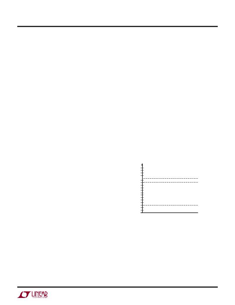
�1.38V�
�1.24V�
�0.3V�
�(NORMAL� OPERATION)�
�(HYSTERESIS� AND� TOLERANCE)�
�LOCKOUT�
�(POWER� SWITCH� OFF,�
�SS� CAPACITOR� DISCHARGED)�
�SHUTDOWN�
�possible,� which� results� in� large� peak� currents.�
�0.0V�
�(LOW� QUIESCENT� CURRENT)�
�3580� F06�
�The� start-up� current� can� be� limited� by� connecting� an�
�external� capacitor� (typically� 100nF� to� 1μF)� to� the� SS� pin.�
�This� capacitor� is� slowly� charged� to� ~2.2V� by� an� internal�
�275k� resistor� once� the� part� is� activated.� SS� pin� voltages�
�below� ~1.1V� reduce� the� internal� current� limit.� Thus,� the�
�gradual� ramping� of� the� SS� voltage� also� gradually� increases�
�the� current� limit� as� the� capacitor� charges.� This,� in� turn,�
�allows� the� output� capacitor� to� charge� gradually� toward� its�
�final� value� while� limiting� the� start-up� current.�
�In� the� event� of� a� commanded� shutdown� or� lockout� (� SHDN�
�pin),� internal� undervoltage� lockout� (UVLO)� or� a� thermal�
�Figure� 6.� Chip� States� vs� SHDN� Voltage�
�Configurable� Undervoltage� Lockout�
�Figure� 7� shows� how� to� configure� an� undervoltage� lockout�
�(UVLO)� for� the� LT3580.� Typically,� UVLO� is� used� in� situations�
�where� the� input� supply� is� current-limited,� has� a� relatively�
�high� source� resistance,� or� ramps� up/down� slowly.� A�
�switching� regulator� draws� constant� power� from� the� source,�
�so� source� current� increases� as� source� voltage� drops.� This�
�looks� like� a� negative� resistance� load� to� the� source� and� can�
�cause� the� source� to� current-limit� or� latch� low� under� low�
�3580fg�
�13�
�相关PDF资料 |
PDF描述 |
|---|---|
| LT3581IMSE#TRPBF | IC REG MULTI CONFIG ADJ 16MSOP |
| LT3582EUD-5#TRPBF | IC REG BOOST INV +/-5V DL 16QFN |
| LT3587EUD#TRPBF | IC REG BOOST INV ADJ DL 20QFN |
| LT3640IFE#TRPBF | IC REG BUCK FIX/ADJ DL 28TSSOP |
| LT3641HFE#TRPBF | IC REG BUCK SYNC ADJ DL 28TSSOP |
相关代理商/技术参数 |
参数描述 |
|---|---|
| LT3581 | 制造商:LINER 制造商全称:Linear Technology 功能描述:3.3A Boost/Inverting DC/DC Converter with Fault Protection |
| LT3581EDE#PBF | 功能描述:IC REG MULTI CONFIG ADJ 14DFN RoHS:是 类别:集成电路 (IC) >> PMIC - 稳压器 - DC DC 开关稳压器 系列:- 标准包装:250 系列:- 类型:降压(降压) 输出类型:固定 输出数:1 输出电压:1.2V 输入电压:2.05 V ~ 6 V PWM 型:电压模式 频率 - 开关:2MHz 电流 - 输出:500mA 同步整流器:是 工作温度:-40°C ~ 85°C 安装类型:表面贴装 封装/外壳:6-UFDFN 包装:带卷 (TR) 供应商设备封装:6-SON(1.45x1) 产品目录页面:1032 (CN2011-ZH PDF) 其它名称:296-25628-2 |
| LT3581EDE#TRPBF | 功能描述:IC REG MULTI CONFIG ADJ 14DFN RoHS:是 类别:集成电路 (IC) >> PMIC - 稳压器 - DC DC 开关稳压器 系列:- 标准包装:2,500 系列:- 类型:降压(降压) 输出类型:固定 输出数:1 输出电压:1.2V,1.5V,1.8V,2.5V 输入电压:2.7 V ~ 20 V PWM 型:- 频率 - 开关:- 电流 - 输出:50mA 同步整流器:是 工作温度:-40°C ~ 125°C 安装类型:表面贴装 封装/外壳:10-TFSOP,10-MSOP(0.118",3.00mm 宽)裸露焊盘 包装:带卷 (TR) 供应商设备封装:10-MSOP 裸露焊盘 |
| LT3581EDE-PBF | 制造商:LINER 制造商全称:Linear Technology 功能描述:3.3A Boost/Inverting DC/DC Converter with Fault Protection |
| LT3581EDE-TRPBF | 制造商:LINER 制造商全称:Linear Technology 功能描述:3.3A Boost/Inverting DC/DC Converter with Fault Protection |
发布紧急采购,3分钟左右您将得到回复。