- 您现在的位置:买卖IC网 > PDF目录1825 > LT3640IFE#TRPBF (Linear Technology)IC REG BUCK FIX/ADJ DL 28TSSOP PDF资料下载
参数资料
| 型号: | LT3640IFE#TRPBF |
| 厂商: | Linear Technology |
| 文件页数: | 10/24页 |
| 文件大小: | 0K |
| 描述: | IC REG BUCK FIX/ADJ DL 28TSSOP |
| 标准包装: | 2,000 |
| 类型: | 降压(降压) |
| 输出类型: | 两者兼有 |
| 输出数: | 2 |
| 输出电压: | 1.8V,3.3V,可调 |
| 输入电压: | 2.5 V ~ 35 V |
| PWM 型: | 电流模式,混合 |
| 频率 - 开关: | 500kHz ~ 2MHz |
| 电流 - 输出: | 1.1A,1.3A |
| 同步整流器: | 无 |
| 工作温度: | -40°C ~ 125°C |
| 安装类型: | 表面贴装 |
| 封装/外壳: | 28-SOIC(0.173",4.40mm 宽)裸露焊盘 |
| 包装: | 带卷 (TR) |
| 供应商设备封装: | 28-TSSOP 裸露焊盘 |
�� �
�
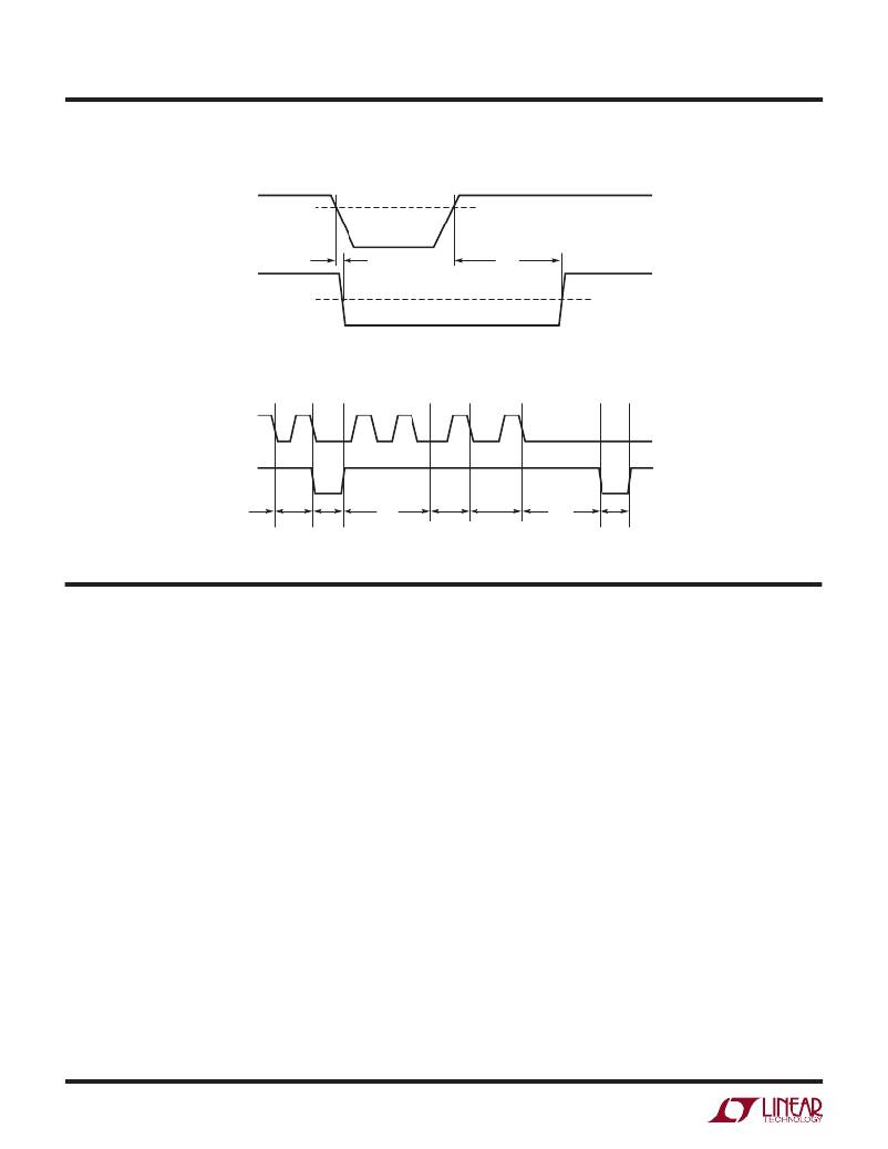
�LT3640�
�TIMING� DIAGRAMS�
�Power-On� Reset� Timing�
�FB�
�RST�
�t� UV�
�t� RST�
�Watchdog� Timing�
�WDI�
�WDO�
�t� DLY�
�t� < t� WD� U�
�t� WDU�
�t� <� t� WDL� t� RST�
�t� WDL� <� t� <� t� WDU�
�t� RST�
�3640� TD�
�OPERATION�
�The� LT3640� is� a� dual� channel,� constant-frequency,� current�
�mode� monolithic� buck� switching� regulator� with� power-on�
�reset� and� watchdog� timer.� Both� channels� are� synchronized�
�to� a� single� oscillator� with� frequency� set� by� RT.� Operation� can�
�be� best� understood� by� referring� to� the� Block� Diagram.�
�Buck� Regulators�
�The� high� voltage� channel� is� a� nonsynchronous� buck�
�regulator� that� operates� from� the� V� IN� pin.� The� start� of� each�
�oscillator� cycle� sets� an� SR� latch� and� turns� on� the� internal�
�NPN� power� switch.� An� amplifier� and� comparator� monitor�
�the� current� flowing� between� the� V� IN� and� SW1� pins,� turning�
�the� switch� off� when� this� current� reaches� a� level� determined�
�by� the� voltage� at� VC1� node.� An� error� amplifier� measures�
�the� output� voltage� through� an� external� resistor� divider� tied�
�to� the� FB1� pin� and� servos� the� VC1� node.� The� reference�
�of� the� error� amplifier� is� determined� by� the� lower� of� the�
�internal� reference� and� the� voltage� at� the� SS1� pin.� If� the� error�
�amplifier’s� output� increases,� more� current� is� delivered� to�
�the� output;� if� it� decreases,� less� current� is� delivered.�
�An� active� clamp� (not� shown)� on� the� VC1� node� provides�
�peak� current� limit.� A� DA� pin� current� comparator� extends�
�the� oscillator� cycle� until� the� catch� diode� current� is� below�
�the� valley� current� limit.� Both� the� peak� and� valley� current�
�limits� help� to� control� the� inductor� current� in� fault� condi-�
�tions� such� as� shorted� output� with� high� V� IN� .� Both� current�
�limits� are� reduced� when� the� voltage� at� the� FB1� pin� is� below�
�0.2V.� This� current� foldback� helps� to� control� the� inductor�
�current� during� start-up� and� overload.�
�The� NPN� power� switch� driver� operates� from� either� the� V� IN�
�pin� or� the� BST� pin.� An� external� capacitor� and� diode� are�
�used� to� generate� a� voltage� between� the� BST� and� SW� pins.�
�During� the� power-up� of� the� LT3640,� an� internal� 5mA� current�
�source� charges� the� external� BST� capacitor.� The� regulator�
�starts� switching� when� the� (BST-SW)� voltage� reaches� the�
�2V� threshold.� The� internal� NPN� power� switch� can� be� fully�
�saturated� for� efficient� operation� when� the� (BST-SW)� volt-�
�age� is� between� 2.3V� and� 5.5V.�
�The� low� voltage� channel� is� a� synchronous� buck� regulator�
�that� operates� from� the� V� IN2� pin.� It� starts� switching� only�
�3640f�
� 0�
�相关PDF资料 |
PDF描述 |
|---|---|
| LT3641HFE#TRPBF | IC REG BUCK SYNC ADJ DL 28TSSOP |
| LT3650IMSE-8.4#TRPBF | IC CHARGER LI-ION 8.4V 2A 12MSOP |
| LT3652EMSE#PBF | IC BATTERY CHARGER SOLAR 12MSOP |
| LT3653IDCB#TRPBF | IC REG BUCK ADJ 1.2A 8DFN |
| LT3663HMS8E-3.3#PBF | IC REG BUCK 3.3V 1.2A 8MSOP |
相关代理商/技术参数 |
参数描述 |
|---|---|
| LT3640IUFD | 制造商:LINER 制造商全称:Linear Technology 功能描述:Dual Monolithic Buck Regulator with Power-On Reset and Watchdog Timer |
| LT3640IUFD#PBF | 功能描述:IC REG BUCK FIX/ADJ DL 28QFN RoHS:是 类别:集成电路 (IC) >> PMIC - 稳压器 - DC DC 开关稳压器 系列:- 设计资源:Design Support Tool 标准包装:1 系列:- 类型:升压(升压) 输出类型:固定 输出数:1 输出电压:3V 输入电压:0.75 V ~ 2 V PWM 型:- 频率 - 开关:- 电流 - 输出:100mA 同步整流器:是 工作温度:-40°C ~ 85°C 安装类型:表面贴装 封装/外壳:SOT-23-5 细型,TSOT-23-5 包装:剪切带 (CT) 供应商设备封装:TSOT-23-5 其它名称:AS1323-BTTT-30CT |
| LT3640IUFD#TRPBF | 功能描述:IC REG BUCK FIX/ADJ DL 28QFN RoHS:是 类别:集成电路 (IC) >> PMIC - 稳压器 - DC DC 开关稳压器 系列:- 设计资源:Design Support Tool 标准包装:1 系列:- 类型:升压(升压) 输出类型:固定 输出数:1 输出电压:3V 输入电压:0.75 V ~ 2 V PWM 型:- 频率 - 开关:- 电流 - 输出:100mA 同步整流器:是 工作温度:-40°C ~ 85°C 安装类型:表面贴装 封装/外壳:SOT-23-5 细型,TSOT-23-5 包装:剪切带 (CT) 供应商设备封装:TSOT-23-5 其它名称:AS1323-BTTT-30CT |
| LT3640IUFDPBF | 制造商:LINER 制造商全称:Linear Technology 功能描述:Dual Monolithic Buck Regulator with Power-On Reset and Watchdog Timer |
| LT3640IUFDTRPBF | 制造商:LINER 制造商全称:Linear Technology 功能描述:Dual Monolithic Buck Regulator with Power-On Reset and Watchdog Timer |
发布紧急采购,3分钟左右您将得到回复。