- 您现在的位置:买卖IC网 > PDF目录16001 > LT3650IMSE-8.2#PBF (Linear Technology)IC CHARGER LI-ION 8.2V 2A 12MSOP PDF资料下载
参数资料
| 型号: | LT3650IMSE-8.2#PBF |
| 厂商: | Linear Technology |
| 文件页数: | 17/22页 |
| 文件大小: | 0K |
| 描述: | IC CHARGER LI-ION 8.2V 2A 12MSOP |
| 标准包装: | 37 |
| 功能: | 充电管理 |
| 电池化学: | 锂离子(Li-Ion)、锂聚合物(Li-Pol) |
| 电源电压: | 9 V ~ 32 V |
| 工作温度: | -40°C ~ 85°C |
| 安装类型: | 表面贴装 |
| 封装/外壳: | 12-TSSOP (0.118",3.00mm 宽)裸露焊盘 |
| 供应商设备封装: | 12-MSOP,裸露焊盘 |
| 包装: | 管件 |
�� �
�
�LT3650-8.2/LT3650-8.4�
�APPLICATIONS� INFORMATION�
�Layout� Considerations�
�The� LT3650� switch� node� has� rise� and� fall� times� that� are�
�typically� less� than� 10ns� to� maximize� conversion� efficiency.�
�The� switched� node� (Pin� SW)� trace� should� be� kept� as� short�
�as� possible� to� minimize� high� frequency� noise.� The� input�
�capacitor� (C� IN� )� should� be� placed� close� to� the� IC� to� minimize�
�this� switching� noise.� Short,� wide� traces� on� these� nodes�
�also� help� to� avoid� voltage� stress� from� inductive� ringing.�
�The� BOOST� decoupling� capacitor� should� also� be� in� close�
�proximity� to� the� IC� to� minimize� inductive� ringing.� The�
�SENSE� and� BAT� traces� should� be� routed� together� and�
�kept� as� short� as� possible.� Shielding� these� signals� from�
�switching� noise� with� ground� is� recommended.�
�High� current� paths� and� transients� should� be� kept� iso-�
�lated� from� battery� ground,� to� assure� an� accurate� output�
�voltage� reference.� Effective� grounding� can� be� achieved�
�by� considering� switched� current� in� the� ground� plane,�
�and� careful� component� placement� and� orientation� can�
�effectively� steer� these� high� currents� such� that� the� battery�
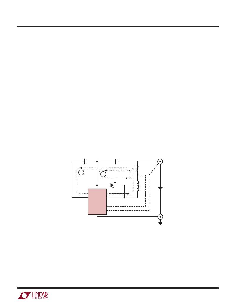
�reference� does� not� get� corrupted.� Figure� 9� illustrates� an�
�effective� grounding� scheme� using� component� placement�
�to� control� ground� currents.� When� the� switch� is� enabled�
�(loop� #1),� current� flows� from� the� input� bypass� capacitor�
�(C� IN� )� through� the� switch� and� inductor� to� the� battery� posi-�
�tive� terminal.� When� the� switch� is� disabled� (loop� #2),� the�
�current� to� the� battery� positive� terminal� is� provided� from�
�ground� through� the� freewheeling� Schottky� diode� (D� F� ).� In�
�both� cases,� these� switched� currents� return� to� ground� via�
�the� output� bypass� capacitor� (C� BAT� ).�
�The� LT3650� packaging� has� been� designed� to� efficiently�
�remove� heat� from� the� IC� via� the� exposed� pad� on� the�
�backside� of� the� package,� which� is� soldered� to� a� copper�
�footprint� on� the� PCB.� This� footprint� should� be� made� as�
�large� as� possible� to� reduce� the� thermal� resistance� of� the�
�IC� case� to� ambient� air.�
�1�
�C� IN�
�V� IN�
�LT3650�
�2�
�SW�
�D� F�
�C� BAT�
�R� SENSE�
�V� BAT�
�+�
�SENSE�
�BAT�
�365082� F09�
�Figure� 9.� Component� Orientation� Isolates� High� Current� Paths� From� Sensitive� Nodes�
�36508284fd�
�17�
�相关PDF资料 |
PDF描述 |
|---|---|
| CCF0.25TB100 | CLEAN CUT FR 1/4" BLK/WHT 100' |
| ACC07DRTF-S13 | CONN EDGECARD 14POS DIP .100 SLD |
| RCC26DRXN | CONN EDGECARD 52POS DIP .100 SLD |
| RCC26DRXH | CONN EDGECARD 52POS DIP .100 SLD |
| RCC17DRTF | CONN EDGECARD 34POS DIP .100 SLD |
相关代理商/技术参数 |
参数描述 |
|---|---|
| LT3651 | 制造商:LINER 制造商全称:Linear Technology 功能描述:High Voltage High Current Controller for Battery Charging and Power Management |
| LT3651-4.1 | 制造商:LINER 制造商全称:Linear Technology 功能描述:Monolithic 4A High Voltage Monolithic 4A High Voltage |
| LT3651-4.2 | 制造商:LINER 制造商全称:Linear Technology 功能描述:Monolithic 4A High Voltage Li-Ion Battery Charger |
| LT3651-8.2 | 制造商:LINER 制造商全称:Linear Technology 功能描述:Monolithic 4A HIgh Voltage 2-Cell Li-Ion Battery Charger |
| LT3651-8.4 | 制造商:LINER 制造商全称:Linear Technology 功能描述:Monolithic 4A HIgh Voltage 2-Cell Li-Ion Battery Charger |
发布紧急采购,3分钟左右您将得到回复。