参数资料
| 型号: | LT3686HDD#TRPBF |
| 厂商: | Linear Technology |
| 文件页数: | 18/28页 |
| 文件大小: | 0K |
| 描述: | IC REG BUCK ADJ 1.2A 10DFN |
| 标准包装: | 2,500 |
| 类型: | 降压(降压) |
| 输出类型: | 可调式 |
| 输出数: | 1 |
| 输出电压: | 0.8 V ~ 30 V |
| 输入电压: | 3.6 V ~ 37 V |
| PWM 型: | 电流模式 |
| 频率 - 开关: | 300kHz ~ 2.5MHz |
| 电流 - 输出: | 1.2A |
| 同步整流器: | 无 |
| 工作温度: | -40°C ~ 150°C |
| 安装类型: | 表面贴装 |
| 封装/外壳: | 10-WFDFN 裸露焊盘 |
| 包装: | 带卷 (TR) |
| 供应商设备封装: | 10-DFN(3x3) |
第1页第2页第3页第4页第5页第6页第7页第8页第9页第10页第11页第12页第13页第14页第15页第16页第17页当前第18页第19页第20页第21页第22页第23页第24页第25页第26页第27页第28页
�� �
�
�LT3686�
�APPLICATIONS� INFORMATION�
�below� the� minimum� voltage� to� sustain� boosted� operation�
�(2.2V� across� the� boost� capacitor),� the� output� voltage� will�
�fall� suddenly� to:�
�V� OUT� =� (V� IN� – 2.2) ? DC� MAX�
�Figure� 9� shows� the� minimum� V� IN� necessary� to� sustain�
�boosted� operation� during� dropout.� Once� V� IN� drops� below�
�the� sustain� voltage,� V� IN� will� need� to� reach� the� start� voltage�
�again� to� refresh� the� boost� capacitor.� The� programmable�
�undervoltage� lockout� (UVLO)� function� can� be� used� to�
�avoid� operating� unless� V� IN� is� greater� than� the� start� voltage.�
�Fixed� Frequency� at� Light� Load�
�The� LT3686� contains� unique� active� load� circuitry� to� allow�
�for� full� frequency� switching� at� very� light� loads.� To� enable�
�the� active� load,� tie� the� MODE� pin� to� greater� than� 0.8V.�
�Typical� fixed� frequency� nonsynchronous� buck� regulators�
�skip� pulses� at� light� loads.� With� a� fixed� input� voltage,� as�
�the� load� current� decreases� in� discontinuous� mode,� the�
�regulator� is� required� to� switch� for� shorter� periods� of� time.�
�When� the� required� on� time� decreases� below� the� typical�
�minimum� on� time,� the� regulator� skips� one� or� more� pulses�
�so� the� effective� average� duty� cycle� is� equal� to� the� required�
�duty� cycle.� This� likelihood� of� entering� pulse-skipping� is�
�exacerbated� by� the� tendency� for� minimum� on� time� to�
�increase� at� very� light� loads.� Pulse-skipping� is� undesirable�
�because� it� causes� unpredictable,� sub-harmonic� output�
�ripple� that� can� interfere� with� the� operation� of� other� sensitive�
�components� such� as� AM� receivers� and� audio� equipment.�
�Instead� of� controlling� switch� current,� the� internal� error�
�amplifier� servos� the� active� load� on� the� output� via� the� BD�
�pin� to� maintain� output� voltage� regulation.� The� impact� on�
�efficiency� is� mitigated� by� pulling� the� minimum� current�
�necessary� to� keep� switching� at� full� frequency.� The� neces-�
�sary� BD� load� to� maintain� output� regulation� depends� on�
�V� IN� ,� inductor� size,� and� load� current.� As� the� necessary�
�BD� load� increases� beyond� its� 40mA� limit,� pulse-skipping�
�mode� will� resume.�
�The� BD� active� load� circuitry� is� enabled� when� MODE� tied�
�high� and� disabled� when� MODE� is� tied� low.� Even� when�
�activated,� the� active� load� will� shutdown� when� BD� voltage�
�exceeds� either� 5.2V� or� V� IN� in� an� effort� to� minimize� power�
�dissipation� and� intelligently� react� to� external� configurations.�
�To� address� the� startup� concerns� delineated� in� the� BOOST�
�and� BD� Pin� Considerations� section,� the� active� load� will�
�assist� startup� by� pulling� maximum� current� (40mA)� to�
�charge� the� boost� capacitor� voltage� in� the� absence� of� an�
�adequate� load.� An� internal� power� good� circuit� will� disable�
�the� BD� active� load� when� V� FB� reaches� 0.7V.� Figure� 9� com-�
�pares� plots� of� minimum� input� voltage� to� start� and� run� as�
�a� function� of� load� current.� In� many� cases� the� discharged�
�output� capacitor� will� present� a� load� to� the� switcher� which�
�will� allow� it� to� start.� The� plots� show� the� worst-case� situ-�
�ation� where� V� IN� is� ramping� very� slowly.�
�The� active� load� also� activates� to� hasten� the� recharge� of�
�boost� cap� when� operating� beyond� maximum� duty� cycle.�
�When� not� in� use,� the� active� load� pulls� no� current.�
�25�
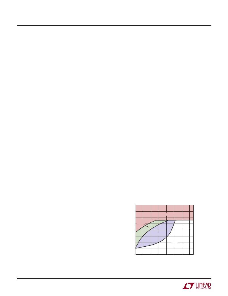
�The� BD� active� load� is� designed� to� combat� pulse-skipping�
�by� providing� an� operational� regime� between� full� frequency�
�discontinuous� and� pulse-skipping� modes.�
�The� maximum� V� IN� before� pulse-skipping� in� discontinu-�
�ous� mode� is� directly� dependent� on� load� current;� as� the�
�load� decreases,� so� does� the� pulse-skipping� boundary.� An�
�artificial� load� on� the� output� helps� push� the� pulse-skipping�
�boundary� higher.� The� LT3686� achieves� this� goal� by� com-�
�manding� the� minimum� load� necessary� to� keep� itself� at�
�full� switching� frequency,� hence� the� circuitry� is� called� an�
�active� load.�
�As� the� LT3686� approaches� minimum� on� time� in� discontinu-�
�ous� mode,� its� power� switch� transitions� smoothly� into� a�
�fixed� on� time,� fixed� frequency� open� loop� current� source.�
�18�
�40�
�35�
�PULSE-SKIPPING�
�30�
�ACTIVE�
�LOAD�
�20�
�D� CM�
�15�
�10� CCM�
�5�
�0�
�0� 20� 40� 60� 80� 100� 120� 140�
�I� OUT� (mA)�
�3686� F10�
�Figure� 10.� Regions� of� Operation� (5V� OUT� ,� 2MHz)�
�3686fc�
�相关PDF资料 |
PDF描述 |
|---|---|
| LT3688HFE#TRPBF | IC REG BUCK ADJ 0.8A DL 24TSSOP |
| LT3689EUD#PBF | IC REG BUCK ADJ 0.7A 16QFN |
| LT3690MPUFE#TRPBF | IC REG BUCK SYNC ADJ 4A 26QFN |
| LT3692IUH#TRPBF | IC REG BUCK ADJ 3.5A DL 32QFN |
| LT3693IMSE#TRPBF | IC REG BUCK ADJ 3.5A 10MSOP |
相关代理商/技术参数 |
参数描述 |
|---|---|
| LT3686IDD | 制造商:LINER 制造商全称:Linear Technology 功能描述:37V/1.2A Step-Down Regulator in 3mm × 3mm DFN |
| LT3686IDD#PBF | 功能描述:IC REG BUCK ADJ 1.2A 10DFN RoHS:是 类别:集成电路 (IC) >> PMIC - 稳压器 - DC DC 开关稳压器 系列:- 标准包装:250 系列:- 类型:降压(降压) 输出类型:固定 输出数:1 输出电压:1.2V 输入电压:2.05 V ~ 6 V PWM 型:电压模式 频率 - 开关:2MHz 电流 - 输出:500mA 同步整流器:是 工作温度:-40°C ~ 85°C 安装类型:表面贴装 封装/外壳:6-UFDFN 包装:带卷 (TR) 供应商设备封装:6-SON(1.45x1) 产品目录页面:1032 (CN2011-ZH PDF) 其它名称:296-25628-2 |
| LT3686IDD#PBF | 制造商:Linear Technology 功能描述:DC-DC CONVERTER BUCK 2.5MHZ 制造商:Linear Technology 功能描述:DC-DC CONVERTER, BUCK, 2.5MHZ, DFN-10 |
| LT3686IDD#TRPBF | 功能描述:IC REG BUCK ADJ 1.2A 10DFN RoHS:是 类别:集成电路 (IC) >> PMIC - 稳压器 - DC DC 开关稳压器 系列:- 标准包装:2,500 系列:- 类型:降压(降压) 输出类型:固定 输出数:1 输出电压:1.2V,1.5V,1.8V,2.5V 输入电压:2.7 V ~ 20 V PWM 型:- 频率 - 开关:- 电流 - 输出:50mA 同步整流器:是 工作温度:-40°C ~ 125°C 安装类型:表面贴装 封装/外壳:10-TFSOP,10-MSOP(0.118",3.00mm 宽)裸露焊盘 包装:带卷 (TR) 供应商设备封装:10-MSOP 裸露焊盘 |
| LT3686IDDPBF | 制造商:LINER 制造商全称:Linear Technology 功能描述:37V/1.2A Step-Down Regulator in 3mm × 3mm DFN |
发布紧急采购,3分钟左右您将得到回复。