参数资料
| 型号: | LT8415IDDB#TRPBF |
| 厂商: | Linear Technology |
| 文件页数: | 7/12页 |
| 文件大小: | 0K |
| 描述: | IC REG BOOST ADJ 25MA 12DFN |
| 标准包装: | 2,500 |
| 类型: | 升压(升压) |
| 输出类型: | 可调式 |
| 输出数: | 1 |
| 输出电压: | 2.5 V ~ 40 V |
| 输入电压: | 2.5 V ~ 16 V |
| PWM 型: | 电流模式 |
| 频率 - 开关: | 800kHz |
| 电流 - 输出: | 25mA |
| 同步整流器: | 无 |
| 工作温度: | -40°C ~ 125°C |
| 安装类型: | 表面贴装 |
| 封装/外壳: | 12-WFDFN 裸露焊盘 |
| 包装: | 带卷 (TR) |
| 供应商设备封装: | 12-DFN-EP(3x2) |
�� �
�
�LT8415�
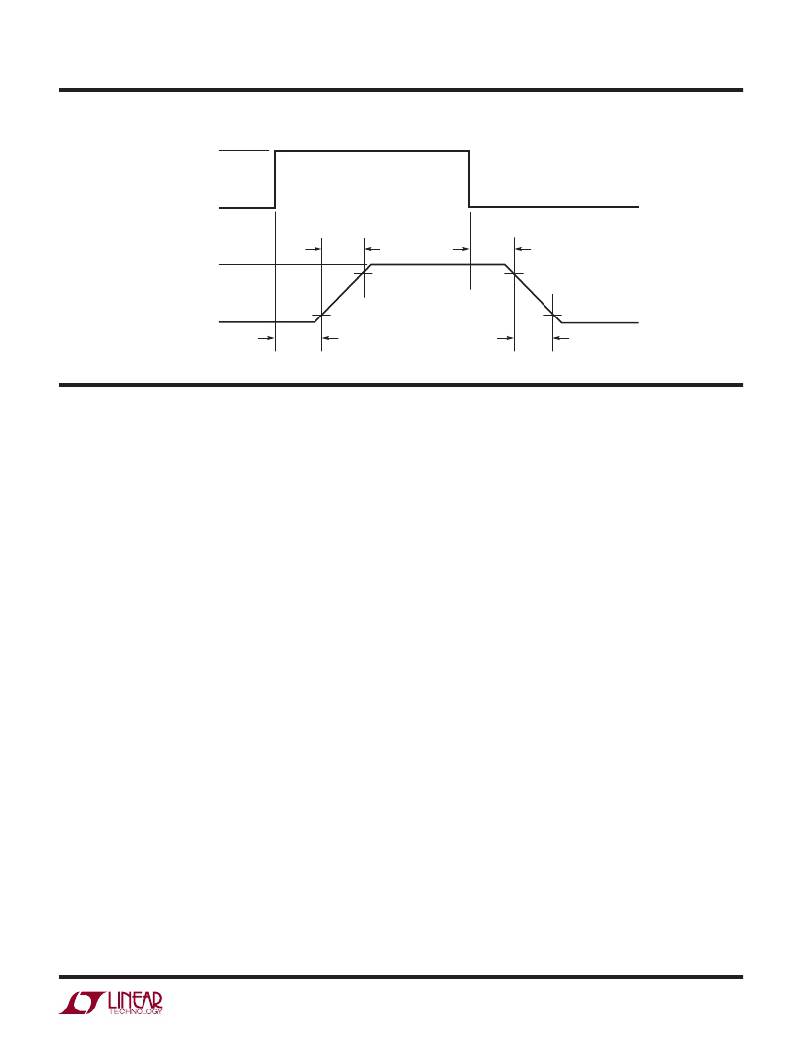
�TIMING� DIAGRAM�
�2V�
�IN1,IN2�
�VOLTAGE�
�0V�
�OUT1,OUT2�
�VOLTAGE�
�34V�
�RISE�
�TIME�
�30V�
�FALL�
�DELAY�
�0V�
�RISE�
�4V�
�FALL�
�OPERATION�
�DELAY�
�TIME�
�8415� TD�
�Switching� Regulator�
�The� LT8415� utilizes� a� variable� peak� current,� variable� off-�
�time� control� scheme� to� provide� high� ef?ciency� over� a� wide�
�output� current� range.�
�The� operation� of� the� part� can� be� better� understood� by�
�referring� to� the� Block� Diagram.� The� part� senses� the�
�output� voltage� by� monitoring� the� internal� FB� node,� and�
�servoing� the� FB� node� voltage� to� be� equal� to� the� FBP�
�pin� voltage.� The� chip� integrates� an� accurate� high� value�
�resistor� divider� (12.4MEG/0.4MEG)� from� the� V� OUT� pin.�
�The� output� voltage� is� set� by� the� FBP� pin� voltage,� which�
�in� turn� is� set� by� an� external� resistor� divider� from� the� V� REF�
�pin.� The� FBP� pin� voltage� can� also� be� directly� biased� with�
�an� external� reference,� allowing� full� control� of� the� output�
�voltage� during� operation.�
�The� Switch� Control� block� senses� the� output� of� the� ampli-�
�?er� and� adjusts� the� switching� frequency� as� well� as� other�
�parameters� to� achieve� regulation.� During� the� start-up� of�
�the� circuit,� special� precautions� are� taken� to� ensure� that�
�the� inductor� current� remains� under� control.�
�The� LT8415� also� has� a� PMOS� output� disconnect� switch.�
�The� PMOS� switch� is� turned� on� when� the� part� is� enabled�
�via� the� SHDN� pin.� When� the� part� is� in� shutdown,� the�
�PMOS� switch� turns� off,� allowing� the� V� OUT� node� to� go� to�
�ground.� This� type� of� disconnect� function� is� often� required�
�in� power� supplies.�
�Half-Bridge�
�The� N-channel� and� P-channel� MOSFETs� in� each� half-bridge�
�are� synchronously� controlled� by� a� single� input� pin,� and�
�will� never� turn� on� at� the� same� time� in� typical� applications,�
�protecting� against� shoot-through� current.� The� OUT1� and�
�OUT2� pins� are� the� same� polarity� as� the� IN1� and� IN2� pins�
�respectively.� When� the� part� is� disabled,� both� N-channel�
�and� P-channel� MOSFETs� turn� off,� and� the� OUT1� and� OUT2�
�pins� will� become� high� impedance� with� a� 20M� pull� down�
�resistor� connected� to� ground.�
�8415f�
�7�
�相关PDF资料 |
PDF描述 |
|---|---|
| LT8582IDKD#TRPBF | IC REG MULTI CONFIG ADJ 3A 24DFN |
| LTC1043CSW#TRPBF | IC BUILDNG BLK SW-CAP DUAL18SOIC |
| LTC1044CS8#TRPBF | IC REG MULTI CONFIG 20MA 8SOIC |
| LTC1046IS8#TRPBF | IC REG SWITCHD CAP DIV INV 8SOIC |
| LTC1142LCG-ADJ#TRPBF | IC REG CTRLR BUCK PWM CM 28-SSOP |
相关代理商/技术参数 |
参数描述 |
|---|---|
| LT8500EUHH#PBF | 功能描述:IC PWM GENERATOR 56-QFN RoHS:是 类别:集成电路 (IC) >> 时钟/计时 - 专用 系列:- 标准包装:1 系列:- 类型:时钟/频率发生器,多路复用器 PLL:是 主要目的:存储器,RDRAM 输入:晶体 输出:LVCMOS 电路数:1 比率 - 输入:输出:1:2 差分 - 输入:输出:无/是 频率 - 最大:400MHz 电源电压:3 V ~ 3.6 V 工作温度:0°C ~ 85°C 安装类型:表面贴装 封装/外壳:16-TSSOP(0.173",4.40mm 宽) 供应商设备封装:16-TSSOP 包装:Digi-Reel® 其它名称:296-6719-6 |
| LT8500EUHH#TRPBF | 功能描述:IC PWM GENERATOR 56-QFN RoHS:是 类别:集成电路 (IC) >> 时钟/计时 - 专用 系列:- 标准包装:28 系列:- 类型:时钟/频率发生器 PLL:是 主要目的:Intel CPU 服务器 输入:时钟 输出:LVCMOS 电路数:1 比率 - 输入:输出:3:22 差分 - 输入:输出:无/是 频率 - 最大:400MHz 电源电压:3.135 V ~ 3.465 V 工作温度:0°C ~ 85°C 安装类型:表面贴装 封装/外壳:64-TFSOP (0.240",6.10mm 宽) 供应商设备封装:64-TSSOP 包装:管件 |
| LT8500IUHH#PBF | 功能描述:IC PWM GENERATOR 56-QFN RoHS:是 类别:集成电路 (IC) >> 时钟/计时 - 专用 系列:- 标准包装:28 系列:- 类型:时钟/频率发生器 PLL:是 主要目的:Intel CPU 服务器 输入:时钟 输出:LVCMOS 电路数:1 比率 - 输入:输出:3:22 差分 - 输入:输出:无/是 频率 - 最大:400MHz 电源电压:3.135 V ~ 3.465 V 工作温度:0°C ~ 85°C 安装类型:表面贴装 封装/外壳:64-TFSOP (0.240",6.10mm 宽) 供应商设备封装:64-TSSOP 包装:管件 |
| LT8500IUHH#TRPBF | 功能描述:IC PWM GENERATOR 56-QFN RoHS:是 类别:集成电路 (IC) >> 时钟/计时 - 专用 系列:- 标准包装:28 系列:- 类型:时钟/频率发生器 PLL:是 主要目的:Intel CPU 服务器 输入:时钟 输出:LVCMOS 电路数:1 比率 - 输入:输出:3:22 差分 - 输入:输出:无/是 频率 - 最大:400MHz 电源电压:3.135 V ~ 3.465 V 工作温度:0°C ~ 85°C 安装类型:表面贴装 封装/外壳:64-TFSOP (0.240",6.10mm 宽) 供应商设备封装:64-TSSOP 包装:管件 |
| LT-8501M | 制造商:Mencom 功能描述: |
发布紧急采购,3分钟左右您将得到回复。