- 您现在的位置:买卖IC网 > PDF目录13904 > LT8582EDKD#TRPBF (Linear Technology)IC REG MULTI CONFIG ADJ 3A 24DFN PDF资料下载
参数资料
| 型号: | LT8582EDKD#TRPBF |
| 厂商: | Linear Technology |
| 文件页数: | 12/36页 |
| 文件大小: | 0K |
| 描述: | IC REG MULTI CONFIG ADJ 3A 24DFN |
| 标准包装: | 2,500 |
| 类型: | 升压(升压),反相,回扫,Sepic |
| 输出类型: | 可调式 |
| 输出数: | 2 |
| 输出电压: | 最高 42V |
| 输入电压: | 2.5 V ~ 22 V |
| PWM 型: | 电流模式 |
| 频率 - 开关: | 200kHz ~ 2.5MHz |
| 电流 - 输出: | 3A |
| 同步整流器: | 无 |
| 工作温度: | -40°C ~ 125°C |
| 安装类型: | 表面贴装 |
| 封装/外壳: | 24-WFDFN 裸露焊盘 |
| 包装: | 带卷 (TR) |
| 供应商设备封装: | 24-DFN(7x4) |
第1页第2页第3页第4页第5页第6页第7页第8页第9页第10页第11页当前第12页第13页第14页第15页第16页第17页第18页第19页第20页第21页第22页第23页第24页第25页第26页第27页第28页第29页第30页第31页第32页第33页第34页第35页第36页
�� �
�
�LT8582�
�OPERATION�
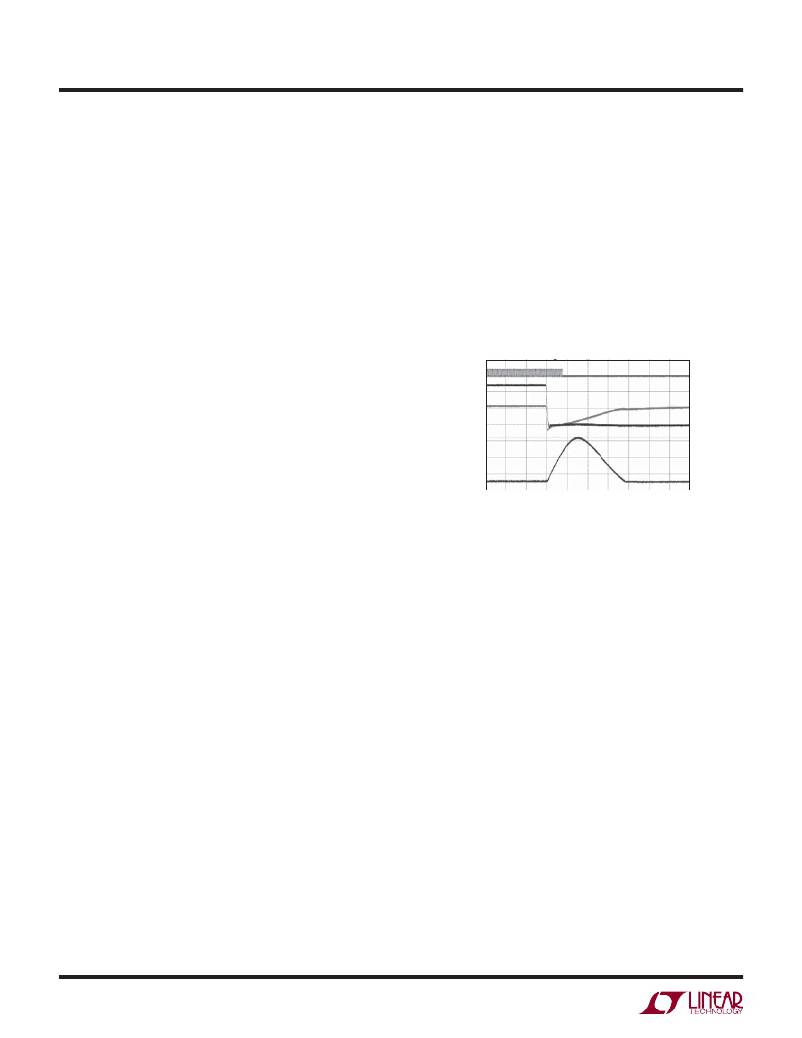
�Refer� to� the� State� Diagram� (Figure� 2)� for� the� following�
�description� of� the� LT8582’s� operation� during� a� fault�
�event.� When� a� fault� is� detected� on� a� channel,� the� LT8582�
�disables� the� CLKOUT� pin� for� that� channel,� turns� off� the�
�power� switches� for� that� channel� and� the� GATE� pin� for� that�
�channel� becomes� high� impedance.� The� external� PMOS,�
�M1,� is� turned� off� by� the� external� R� GATE� resistor� (see�
�Block� Diagram).� With� the� external� PMOS� turned� off,� the�
�power� path� from� V� IN� to� V� OUT� is� opened,� protecting�
�power� path� components.� Also,� as� soon� as� the� feedback�
�voltage� falls� inside� the� range� 65mV� <� FBX� <� 1.15V,� PG�
�OPERATION� –� CURRENT� LIMIT�
�The� current� limit� operates� independently� of� the� FAULT�
�current� limit.� The� current� limit� sets� a� maximum� switch�
�current.� This� switch� current� limit� is� duty� cycle� dependent,�
�but� for� most� applications� will� be� around� 3A� minimum� (see�
�the� Electrical� Characteristics).� Once� this� limit� is� reached,�
�the� switch� duty� cycle� decreases,� reducing� the� magnitude�
�of� the� output� voltage.� If,� despite� the� reduced� duty� cycle�
�the� switch� current� reaches� the� FAULT� current� limit,� the� part�
�will� behave� as� described� in� the� Operation� –� Fault� section.�
�pulls� low.� Refer� to� Figure� 4� for� the� case� of� an� output� short.�
�CLKOUT�
�At� the� beginning� of� a� fault� event,� a� timeout� sequence� com-�
�mences� where� the� SS� pin� for� that� channel� is� charged� up� to�
�1.84V� (the� SS� pin� will� continue� charging� up� to� ~2.1V� and�
�be� held� there� in� the� case� of� a� FAULT� event� that� still� exists)�
�and� then� discharged� to� 55mV.� This� timeout� period� relieves�
�the� chip,� the� PMOS� and� other� power� path� components�
�5V/DIV�
�V� OUT1�
�5V/DIV�
�GATE�
�5V/DIV�
�I� L1�
�5A/DIV�
�from� electrical� and� thermal� stress� for� a� minimum� amount�
�of� time� set� by� the� voltage� ramp� rate� on� the� SS� pin.�
�20μs/DIV�
�8582� F04�
�Figure� 4.� Output� Short-Circuit� Protection� of� the� LT8582�
�8582f�
�12�
�相关PDF资料 |
PDF描述 |
|---|---|
| RCM31DCSD-S288 | CONN EDGECARD 62POS .156 EXTEND |
| HM100-251R0LFTR13 | HIGH CURR LOW PROFILE INDUCTORS |
| RBM24DCSD-S288 | CONN EDGECARD 48POS .156 EXTEND |
| LT1534IS | IC REG BOOST ADJ 2A 16SOIC |
| HM53-40111VLF | HIGH POWER LOW COST INDUCTORS |
相关代理商/技术参数 |
参数描述 |
|---|---|
| LT8582IDKD#PBF | 功能描述:IC REG MULTI CONFIG ADJ 3A 24DFN RoHS:是 类别:集成电路 (IC) >> PMIC - 稳压器 - DC DC 开关稳压器 系列:- 标准包装:250 系列:- 类型:降压(降压) 输出类型:固定 输出数:1 输出电压:1.2V 输入电压:2.05 V ~ 6 V PWM 型:电压模式 频率 - 开关:2MHz 电流 - 输出:500mA 同步整流器:是 工作温度:-40°C ~ 85°C 安装类型:表面贴装 封装/外壳:6-UFDFN 包装:带卷 (TR) 供应商设备封装:6-SON(1.45x1) 产品目录页面:1032 (CN2011-ZH PDF) 其它名称:296-25628-2 |
| LT8582IDKD#PBF | 制造商:Linear Technology 功能描述:DC/DC CONVRTER BOOST INVERTING SEPIC |
| LT8582IDKD#TRPBF | 功能描述:IC REG MULTI CONFIG ADJ 3A 24DFN RoHS:是 类别:集成电路 (IC) >> PMIC - 稳压器 - DC DC 开关稳压器 系列:- 设计资源:Design Support Tool 标准包装:1 系列:- 类型:升压(升压) 输出类型:固定 输出数:1 输出电压:3V 输入电压:0.75 V ~ 2 V PWM 型:- 频率 - 开关:- 电流 - 输出:100mA 同步整流器:是 工作温度:-40°C ~ 85°C 安装类型:表面贴装 封装/外壳:SOT-23-5 细型,TSOT-23-5 包装:剪切带 (CT) 供应商设备封装:TSOT-23-5 其它名称:AS1323-BTTT-30CT |
| LT8584IFE#PBF | 制造商:Linear Technology 功能描述:IC BATT CELL BALANCE 16TSSOP 制造商:Linear Technology 功能描述:BATTERY BALANCER, 2.5V-5.3V, TSSOP-16, Supply Voltage Min:2.5V, Supply Voltage M |
| LT8610 | 制造商:LINER 制造商全称:Linear Technology 功能描述:42V, 2.5A Synchronous Step-Down Regulator |
发布紧急采购,3分钟左右您将得到回复。