- 您现在的位置:买卖IC网 > PDF目录1826 > LT8582IDKD#TRPBF (Linear Technology)IC REG MULTI CONFIG ADJ 3A 24DFN PDF资料下载
参数资料
| 型号: | LT8582IDKD#TRPBF |
| 厂商: | Linear Technology |
| 文件页数: | 13/36页 |
| 文件大小: | 0K |
| 描述: | IC REG MULTI CONFIG ADJ 3A 24DFN |
| 标准包装: | 2,500 |
| 类型: | 升压(升压),反相,回扫,Sepic |
| 输出类型: | 可调式 |
| 输出数: | 2 |
| 输出电压: | 最高 42V |
| 输入电压: | 2.5 V ~ 22 V |
| PWM 型: | 电流模式 |
| 频率 - 开关: | 200kHz ~ 2.5MHz |
| 电流 - 输出: | 3A |
| 同步整流器: | 无 |
| 工作温度: | -40°C ~ 125°C |
| 安装类型: | 表面贴装 |
| 封装/外壳: | 24-WFDFN 裸露焊盘 |
| 包装: | 带卷 (TR) |
| 供应商设备封装: | 24-DFN(7x4) |
第1页第2页第3页第4页第5页第6页第7页第8页第9页第10页第11页第12页当前第13页第14页第15页第16页第17页第18页第19页第20页第21页第22页第23页第24页第25页第26页第27页第28页第29页第30页第31页第32页第33页第34页第35页第36页
�� ��
��
��LT8582�
�APPLICATIONS� INFORMATION�
�Boost� Converter� Component� Selection�
�Table� 1.� Boost� Converter� Design� Equations�
�V� OUT� –� V� IN� +� 0.5V�
�V� OUT� +� 0.5V� –� 0.3V�
�V� IN�
�5V�
�L1�
�4.7μH�
�SWA�
�D1�
�30V,� 2A�
�SWB�
�C� OUT1�
�10μF�
�R� FBX�
�130k�
�OPTIONAL�
�M1�
�6.04k�
�V� OUT�
�12V�
�0.8A�
�Step� 1:� Inputs�
�Step� 2:� DC�
�PARAMETERS/EQUATIONS�
�Choose� V� IN� ,� V� OUT� and� f� OSC� to� calculate� equations�
�below.�
�DC� ?�
�215k�
�100k�
�V� IN� FBX�
�LT8582�
�SHDN� CHx� GATE�
�PG� CLKOUT�
�C� OUT2�
�10μF�
�Step� 3:� L1�
�L� TYP� =�
�(V� IN� – 0.3) ? DC�
�f� OSC� ?� 1A�
�(1)�
�C� IN�
�4.7μF�
�R� T�
�53.6k�
�RT�
�SYNC� GND�
�V� C�
�SS�
�47pF�
�6.49k�
�L� MIN� =�
�(V� IN� – 0.3V) ? (2 ? DC – 1)�
�1.7A� ?� f� OSC� ?� (1� –� DC)�
�(2)�
�0.1μF�
�4.7nF�
�8582� F05�
�L� MAX� =�
�(V� IN� – 0.3V) ? DC�
�f� OSC� ?� 0.18A�
�(3)�
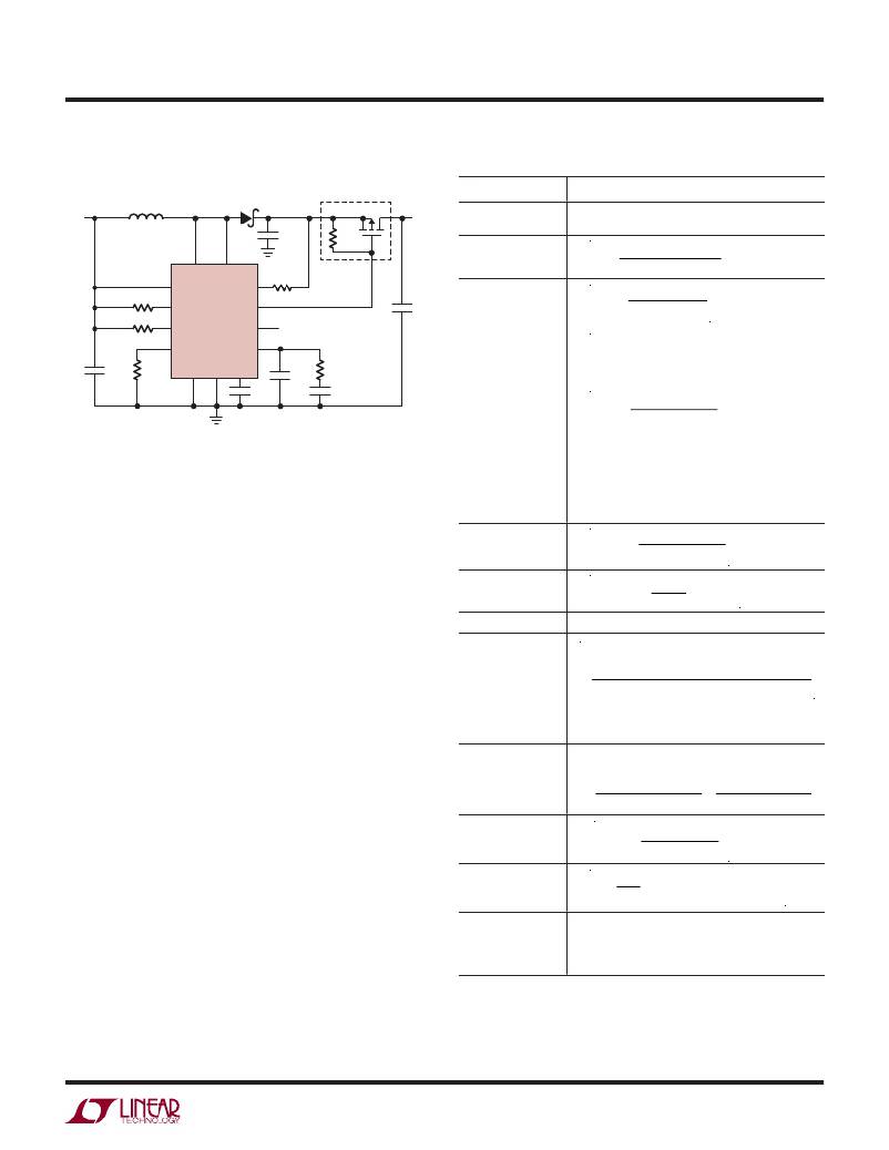
�Figure� 5.� Boost� Converter� –� The� Component� Values� Given�
�Are� Typical� Values� for� a� 1.5MHz,� 5V� to� 12V� Boost�
�Each� channel� of� the� LT8582� can� be� configured� as� a� boost�
�converter� as� in� Figure� 5.� This� topology� allows� for� positive�
�?� Solve� equations� 1,� 2� and� 3� for� a� range� of� L�
�values�
�?� The� minimum� of� the� L� value� range� is� the�
�higher� of� L� TYP� and� L� MIN�
�?� The� maximum� of� the� L� value� range� is� L� MAX�
�output� voltages� that� are� higher� than� the� input� voltage.� An�
�external� PMOS� (optional)� driven� by� the� GATE� pin� of� the�
�Step� 4:� I� RIPPLE�
�I� RIPPLE� =�
�(V� IN� – 0.3V) ? DC�
�f� OSC� ?� L� 1�
�I� OUT� =� ?� 3A� –�
�LT8582 can achieve input or output disconnect during a�
�FAULT� event,� SHDN� <� 1.31V,� or� V� IN� <� 2.3V.� Figure� 5� shows�
�the� configuration� for� output� disconnect.� A� single� feedback�
�resistor� sets� the� output� voltage.� For� output� voltages� higher�
�than� 40V,� see� the� Charge� Pump� Topology� in� the� Charge�
�Pump� Aided� Regulators� section.�
�Table� 1� is� a� step-by-step� set� of� equations� to� calculate�
�component� values� for� the� LT8582� when� operating� as� a�
�boost� converter.� Input� parameters� are� input� and� output�
�voltage� and� switching� frequency� (V� IN� ,� V� OUT� and� f� OSC� re-�
�Step� 5:� I� OUT�
�Step� 6:� D1�
�Step� 7:� C� OUT�
�Step� 8:� C� IN�
�?� I� RIPPLE� ?�
�?�
�?� 2� ?� ?� (1� –� DC)�
�V� R� ≥� V� OUT� ;� I� AVG� ≥� I� OUT�
�C� OUT1� C� OUT2�
�I� OUT� DC�
�f� OSC� (0.01� V� OUT� –� 0.5� I� OUT� R� DSON� _� PMOS� )�
�?� If� PMOS� is� not� used,� then� use� just� one�
�capacitor� where� C� OUT� =� C� OUT1� +� C� OUT2�
�C� IN� C� VIN� C� PWR�
�spectively).� Refer� to� the� Appendix� for� further� information�
�on� the� design� equations� presented� in� Table� 1.�
�3A� DC�
�50� f� OSC� 0.005� V� IN�
�I� RIPPLE�
�8� f� OSC� 0.005� V� IN�
�R� FBX� =� ?� OUT�
�Variable Definitions:�
�V� IN� =� Input� Voltage�
�Step� 9:� R� FBX�
�?� V – 1.204V� ?�
�?�
�?� 83.3μA� ?�
�V� OUT� =� Output� Voltage�
�DC� =� Power� Switch� Duty� Cycle�
�Step� 10:� R� T�
�R� T� =�
�81.6�
�f� OSC�
�–1;� f� OSC� in� MHz� and� R� T� in� k� Ω�
�f� OSC� =� Switching� Frequency�
�I� OUT� =� Maximum� Output� Current�
�I� RIPPLE� =� Inductor� Ripple� Current�
�R� DSON_PMOS� =� R� DSON� of� External� Output� PMOS� (set� to� 0�
�if� not� using� PMOS)�
�Step� 11:� PMOS� Only� needed� for� input� or� output� disconnect.� See�
�PMOS� Selection� in� the� Appendix� for� information�
�on� sizing� the� PMOS� and� the� biasing� resistor,�
�R� GATE� and� picking� appropriate� UVLO� components.�
�Note� 1:� Above� equations� use� numbers� good� for� many� applications� but�
�for� more� exact� results� use� the� equations� from� the� appendix� with� numbers�
�from� the� Electrical� Characteristics.�
�Note� 2:� The� final� values� for� C� OUT1� ,� C� OUT2� and� C� IN� may� deviate� from� the�
�above� equations� in� order� to� obtain� desired� load� transient� performance.�
�8582f�
�13�
�相关PDF资料 |
PDF描述 |
|---|---|
| LTC1043CSW#TRPBF | IC BUILDNG BLK SW-CAP DUAL18SOIC |
| LTC1044CS8#TRPBF | IC REG MULTI CONFIG 20MA 8SOIC |
| LTC1046IS8#TRPBF | IC REG SWITCHD CAP DIV INV 8SOIC |
| LTC1142LCG-ADJ#TRPBF | IC REG CTRLR BUCK PWM CM 28-SSOP |
| LTC1143LCS#PBF | IC REG CTRLR BUCK PWM CM 16-SOIC |
相关代理商/技术参数 |
参数描述 |
|---|---|
| LT8584IFE#PBF | 制造商:Linear Technology 功能描述:IC BATT CELL BALANCE 16TSSOP 制造商:Linear Technology 功能描述:BATTERY BALANCER, 2.5V-5.3V, TSSOP-16, Supply Voltage Min:2.5V, Supply Voltage M |
| LT8610 | 制造商:LINER 制造商全称:Linear Technology 功能描述:42V, 2.5A Synchronous Step-Down Regulator |
| LT8610ABEMSE#PBF | 制造商:Linear Technology 功能描述:SWITCHING REG, BUCK, ADJ, 2.2MHZ, MSOP16, Primary Input Voltage:42V, No. of Outp |
| LT8610AEMSE#PBF | 制造商:Linear Technology 功能描述:IC REG BUCK SYNC ADJ 2.5A 16MSOP 制造商:Linear Technology 功能描述:SWITCHING REG, BUCK, ADJ, 2.2MHZ, MSOP16, Primary Input Voltage:42V, No. of Outp |
| LT8610AHMSE#PBF | 制造商:Linear Technology 功能描述:IC REG BUCK SYNC ADJ 2.5A 16MSOP 制造商:Linear Technology 功能描述:SWITCHING REG, BUCK, ADJ, 2.2MHZ, MSOP16 制造商:Linear Technology 功能描述:SWITCHING REG, BUCK, ADJ, 2.2MHZ, MSOP16, Primary Input Voltage:42V, No. of Outp |
发布紧急采购,3分钟左右您将得到回复。