- 您现在的位置:买卖IC网 > PDF目录9480 > LTC1092ACN8#PBF (Linear Technology)IC DAS SERIAL I/O 1CH 10BIT 8DIP PDF资料下载
参数资料
| 型号: | LTC1092ACN8#PBF |
| 厂商: | Linear Technology |
| 文件页数: | 11/32页 |
| 文件大小: | 0K |
| 描述: | IC DAS SERIAL I/O 1CH 10BIT 8DIP |
| 标准包装: | 50 |
| 类型: | 数据采集系统(DAS),ADC |
| 分辨率(位): | 10 b |
| 数据接口: | 串行 |
| 电压电源: | 双 ± |
| 电源电压: | ±5V,4.5V,10V |
| 工作温度: | -40°C ~ 85°C |
| 安装类型: | 通孔 |
| 封装/外壳: | 8-DIP(0.300",7.62mm) |
| 供应商设备封装: | 8-PDIP |
| 包装: | 管件 |
第1页第2页第3页第4页第5页第6页第7页第8页第9页第10页当前第11页第12页第13页第14页第15页第16页第17页第18页第19页第20页第21页第22页第23页第24页第25页第26页第27页第28页第29页第30页第31页第32页
19
LTC1091/LTC1092
LTC1093/LTC1094
U
S
A
O
PPLICATI
WU
U
I FOR ATIO
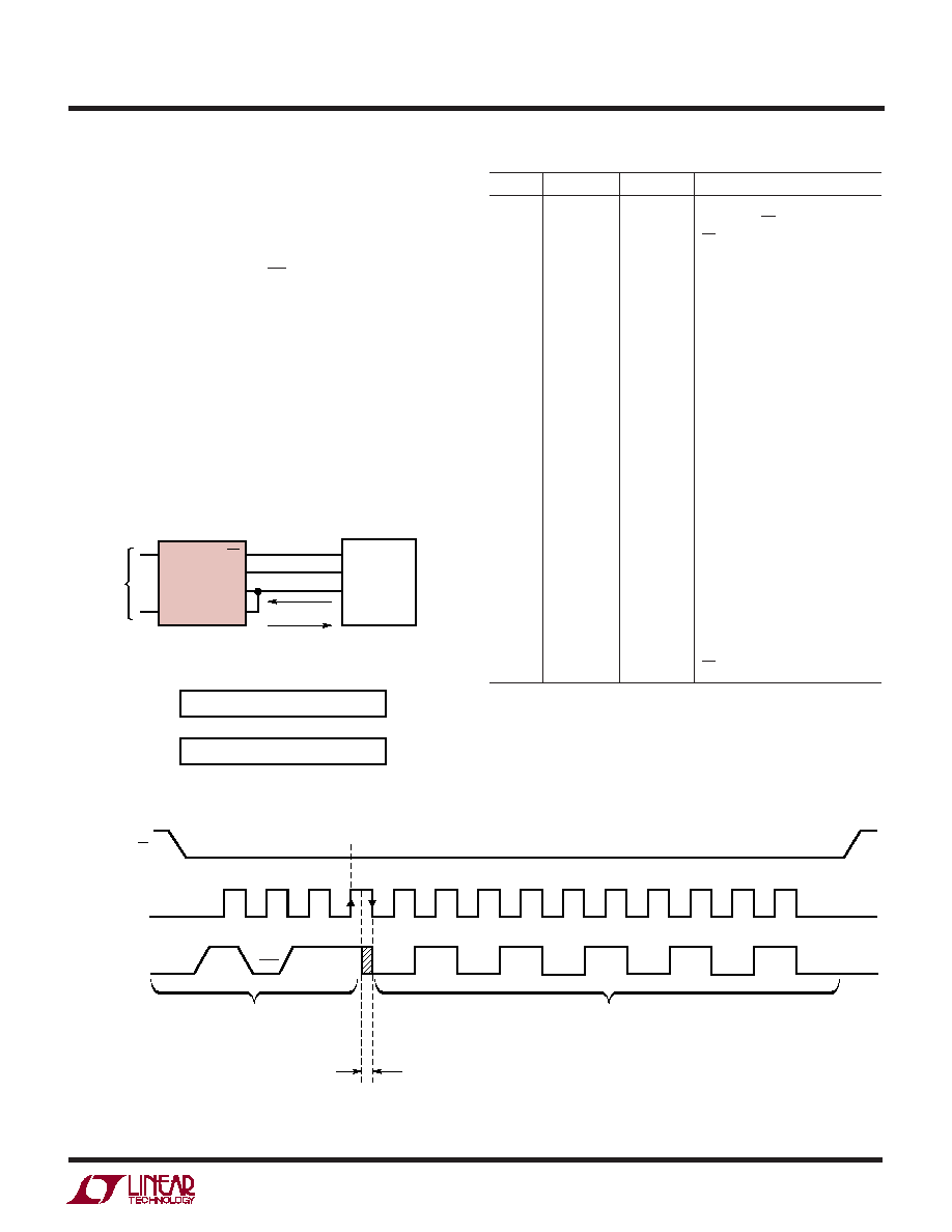
Interfacing to the Parallel Port of the
Intel 8051 Family
The Intel 8051 has been chosen to demonstrate the
interface between the LTC1091 and parallel port micro-
processors. Normally, the CS, SCLK and DIN signals
would be generated on three port lines and the DOUT signal
read on a 4th port line. This works very well. However, we
will demonstrate here an interface with the DIN and DOUT
of the LTC1091 tied together as described in section 4.
This saves one wire.
The 8051 first sends the start bit and MUX address to the
LTC1091 over the data line connected to P1.2. Then P1.2
is reconfigured as an input (by writing to it a one) and the
8051 reads back the 10-bit A/D result over the same data
line.
1091-4 AI17
LTC1091
CS
CLK
DOUT
DIN
ANALOG
INPUTS
P1.4
P1.3
P1.2
8051
MUX ADDRESS
A/D RESULT
B9
B8
B7
B6
B5
B4
B3
B2
DOUT from LTC1091 Stored in 8051 RAM
MSB
R2
B1
B0
0
LSB
R3
LABEL
MNEMONIC
OPERAND
COMMENTS
MOV
A, #FFH
DIN Word for LTC1091
SETB
P1.4
Make Sure CS Is High
CLR
P1.4
CS Goes Low
MOV
R4, #04
Load Counter
LOOP 1 RLC
A
Rotate DIN Bit into Carry
CLR
P1.3
SCLK Goes Low
MOV
P1.2, C
Output DIN Bit to LTC1091
SETB
P1.3
SCLK Goes High
DJNZ
R4, LOOP 1
Next Bit
MOV
P1, #04
Bit 2 Becomes an Input
CLR
P1.3
SCLK Goes Low
MOV
R4, #09
Load Counter
LOOP
MOV
C, P1.2
Read Data Bit into Carry
RLC
A
Rotate Data Bit into Acc
SETB
P1.3
SCLK Goes High
CLR
P1.3
SCLK Goes Low
DJNZ
R4, LOOP
Next Bit
MOV
R2, A
Store MSBs in R2
MOV
C, P1.2
Read Data Bit into Carry
SETB
P1.3
SCLK Goes High
CLR
P1.3
SCLK Goes Low
CLR
A
Clear Acc
RLC
A
Rotate Data Bit from Carry to Acc
MOV
C, P1.2
Read Data Bit into Carry
RRC
A
Rotate Right into Acc
RRC
A
Rotate Right into Acc
MOV
R3, A
Store LSBs in R3
SETB
P1.4
CS Goes High
1091/2/3/4 AI18
CLK
START
MSBF
B9
B8
B7
B6
B5
B4
B3
B2
B1
B0
8051 P1.2 RECONFIGURED AS AN
INPUT AFTER THE 4TH RISING CLK
AND BEFORE THE 4TH FALLING CLK
8051 P1.2 OUTPUTS
DATA TO LTC1091
LTC1091 TAKES CONTROL OF DATA LINE
ON 4TH FALLING CLK
SGL/
DIFF
ODD/
SIGN
CS
DATA (DIN/DOUT)
12
MSBF BIT
LATCHED
INTO LTC1091
3
4
LTC1091 SENDS A/D RESULT
BACK TO 8051 P1.2
相关PDF资料 |
PDF描述 |
|---|---|
| LTC1092ACN8 | IC DAS SERIAL I/O 1CH 10BIT 8DIP |
| LTC1091ACN8#PBF | IC DATA ACQ SYS 10BIT 2CH 8-DIP |
| LTC1091ACN8 | IC DATA ACQ SYS 10BIT 2CH 8-DIP |
| AD7729ARUZ | IC ADC 15BIT DUAL W/DAC 28TSSOP |
| AD7729ARZ | IC ADC 15BIT DUAL W/DAC 28SOIC |
相关代理商/技术参数 |
参数描述 |
|---|---|
| LTC1092AMJ8 | 制造商:未知厂家 制造商全称:未知厂家 功能描述:Analog-to-Digital Converter, 10-Bit |
| LTC1092AMJ8/883 | 制造商:Linear Technology 功能描述: |
| LTC1092C | 制造商:LINER 制造商全称:Linear Technology 功能描述:1-, 2-, 6- and 8-Channel, 10-Bit Serial I/O Data Acquisition Systems |
| LTC1092CJ8 | 制造商:未知厂家 制造商全称:未知厂家 功能描述:Analog-to-Digital Converter, 10-Bit |
| LTC1092CN8 | 功能描述:IC DAS SERIAL I/O 1CH 10BIT 8DIP RoHS:否 类别:集成电路 (IC) >> 数据采集 - ADCs/DAC - 专用型 系列:- 产品培训模块:Lead (SnPb) Finish for COTS Obsolescence Mitigation Program 标准包装:50 系列:- 类型:数据采集系统(DAS) 分辨率(位):16 b 采样率(每秒):21.94k 数据接口:MICROWIRE?,QSPI?,串行,SPI? 电压电源:模拟和数字 电源电压:1.8 V ~ 3.6 V 工作温度:-40°C ~ 85°C 安装类型:表面贴装 封装/外壳:40-WFQFN 裸露焊盘 供应商设备封装:40-TQFN-EP(6x6) 包装:托盘 |
发布紧急采购,3分钟左右您将得到回复。