- 您现在的位置:买卖IC网 > PDF目录9480 > LTC1092ACN8#PBF (Linear Technology)IC DAS SERIAL I/O 1CH 10BIT 8DIP PDF资料下载
参数资料
| 型号: | LTC1092ACN8#PBF |
| 厂商: | Linear Technology |
| 文件页数: | 31/32页 |
| 文件大小: | 0K |
| 描述: | IC DAS SERIAL I/O 1CH 10BIT 8DIP |
| 标准包装: | 50 |
| 类型: | 数据采集系统(DAS),ADC |
| 分辨率(位): | 10 b |
| 数据接口: | 串行 |
| 电压电源: | 双 ± |
| 电源电压: | ±5V,4.5V,10V |
| 工作温度: | -40°C ~ 85°C |
| 安装类型: | 通孔 |
| 封装/外壳: | 8-DIP(0.300",7.62mm) |
| 供应商设备封装: | 8-PDIP |
| 包装: | 管件 |
第1页第2页第3页第4页第5页第6页第7页第8页第9页第10页第11页第12页第13页第14页第15页第16页第17页第18页第19页第20页第21页第22页第23页第24页第25页第26页第27页第28页第29页第30页当前第31页第32页
8
LTC1091/LTC1092
LTC1093/LTC1094
LTC1092/LTC1093/LTC1094
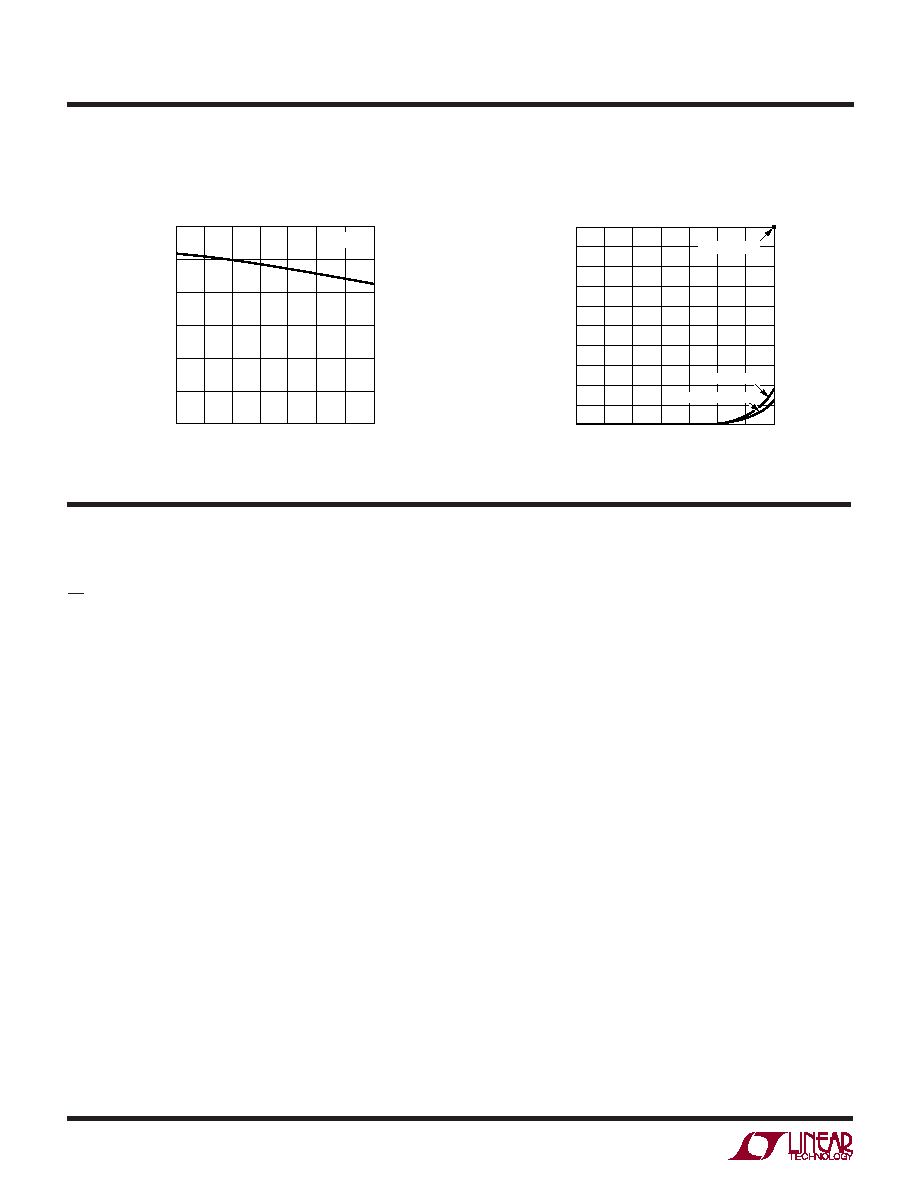
Reference Current vs Temperature
AMBIENT TEMPERATURE (
°C)
–50
REFERENCE
CURRENT
(mA)
0.6
0.5
0.4
0.3
0.2
0.1
0
50
1091/2/3/4 G28
–25
0
25
75
125
100
VREF = 5V
AMBIENT TEMPERATURE (
°C)
–50
0
INPUT
CHANNEL
LEAKAGE
CURRENT
(nA)
100
300
400
500
1000
700
0
25
50
125
1091/2/3/4 G29
200
800
900
600
–25
75
100
ON-CHANNEL
OFF-CHANNEL
GUARANTEED
LTC1093/LTC1094 Input Channel
Leakage Current vs Temperature
PI FU CTIO S
U
UU
LTC1091/LTC1092
CS (Pin 1): Chip Select Input. A logic low on this input
enables the LTC1091/LTC1092.
CH0, CH1/+ IN, – IN (Pins 2, 3): Analog Inputs. These
inputs must be free of noise with respect to GND.
GND (Pin 4): Analog Ground. GND should be tied directly
to an analog ground plane.
DIN (Pin 5)(LTC1091): Digital Data Input. The multiplexer
address is shifted into this input.
VREF (Pin 5)(LTC1092): Reference Input. The reference
input defines the span of the A/D converter and must be
kept free of noise with respect to AGND.
DOUT (Pin 6): Digital Data Output. The A/D conversion
result is shifted out of this output.
CLK (Pin 7): Shift Clock. This clock synchronizes the serial
data transfer.
VCC(VREF)(Pin 8)(LTC1091): Positive Supply and Refer-
ence Voltage. This pin provides power and defines the
span of the A/D converter. It must be kept free of noise and
ripple by bypassing directly to the analog ground plane.
VCC (Pin 8 )(LTC1092): Positive Supply Voltage. This pin
provides power to the A/D converter. It must be kept free
of noise and ripple by bypassing directly to the analog
ground plane.
LTC1093/LTC1094
CH0 to CH5/CH0 to CH7 (Pins 1 to 6/Pins 1 to 8): Analog
Inputs. The analog inputs must be free of noise with
respect to AGND.
COM (Pin 7/Pin 9): Common. The common pin defines the
zero reference point for all single-ended inputs. It must be
free of noise and is usually tied to the analog ground plane.
DGND (Pin 8/Pin 10): Digital Ground. This is the ground
for the internal logic. Tie to the ground plane.
V – (Pin 9/Pin 11): Negative Supply. Tie V – to most
negative potential in the circuit. (Ground in single supply
applications.)
AGND (Pin 10/Pin 12): Analog Ground. AGND should be
tied directly to the analog ground plane.
CC
HARA TERISTICS
UW
A
TYPICALPERFOR
CE
相关PDF资料 |
PDF描述 |
|---|---|
| LTC1092ACN8 | IC DAS SERIAL I/O 1CH 10BIT 8DIP |
| LTC1091ACN8#PBF | IC DATA ACQ SYS 10BIT 2CH 8-DIP |
| LTC1091ACN8 | IC DATA ACQ SYS 10BIT 2CH 8-DIP |
| AD7729ARUZ | IC ADC 15BIT DUAL W/DAC 28TSSOP |
| AD7729ARZ | IC ADC 15BIT DUAL W/DAC 28SOIC |
相关代理商/技术参数 |
参数描述 |
|---|---|
| LTC1092AMJ8 | 制造商:未知厂家 制造商全称:未知厂家 功能描述:Analog-to-Digital Converter, 10-Bit |
| LTC1092AMJ8/883 | 制造商:Linear Technology 功能描述: |
| LTC1092C | 制造商:LINER 制造商全称:Linear Technology 功能描述:1-, 2-, 6- and 8-Channel, 10-Bit Serial I/O Data Acquisition Systems |
| LTC1092CJ8 | 制造商:未知厂家 制造商全称:未知厂家 功能描述:Analog-to-Digital Converter, 10-Bit |
| LTC1092CN8 | 功能描述:IC DAS SERIAL I/O 1CH 10BIT 8DIP RoHS:否 类别:集成电路 (IC) >> 数据采集 - ADCs/DAC - 专用型 系列:- 产品培训模块:Lead (SnPb) Finish for COTS Obsolescence Mitigation Program 标准包装:50 系列:- 类型:数据采集系统(DAS) 分辨率(位):16 b 采样率(每秒):21.94k 数据接口:MICROWIRE?,QSPI?,串行,SPI? 电压电源:模拟和数字 电源电压:1.8 V ~ 3.6 V 工作温度:-40°C ~ 85°C 安装类型:表面贴装 封装/外壳:40-WFQFN 裸露焊盘 供应商设备封装:40-TQFN-EP(6x6) 包装:托盘 |
发布紧急采购,3分钟左右您将得到回复。