- 您现在的位置:买卖IC网 > PDF目录15253 > LTC1159IS-5#TR (Linear Technology)IC REG CTRLR BUCK PWM CM 16-SOIC PDF资料下载
参数资料
| 型号: | LTC1159IS-5#TR |
| 厂商: | Linear Technology |
| 文件页数: | 10/20页 |
| 文件大小: | 0K |
| 描述: | IC REG CTRLR BUCK PWM CM 16-SOIC |
| 标准包装: | 2,500 |
| PWM 型: | 电流模式 |
| 输出数: | 1 |
| 频率 - 最大: | 250kHz |
| 占空比: | 100% |
| 电源电压: | 4 V ~ 40 V |
| 降压: | 是 |
| 升压: | 无 |
| 回扫: | 无 |
| 反相: | 无 |
| 倍增器: | 无 |
| 除法器: | 无 |
| Cuk: | 无 |
| 隔离: | 无 |
| 工作温度: | -40°C ~ 85°C |
| 封装/外壳: | 16-SOIC(0.154",3.90mm 宽) |
| 包装: | 带卷 (TR) |
| 其它名称: | LTC1159IS-5TR LTC1159IS5TR |
�� �
�
�LTC1159�
�LTC1159-3.3/LTC1159-5�
�APPLICATIO� S� I� FOR� ATIO�
�C� IN� Required� I� RMS� ≈� MAX�
�C� IN� and C� OUT� Selection�
�In� continuous� mode,� the� source� current� of� the� P-channel�
�MOSFET� is� a� square� wave� of� duty� cycle� V� OUT� /V� IN� .�
�To� prevent� large� voltage� transients,� a� low� ESR� input�
�capacitor� sized� for� the� maximum� RMS� current� must� be�
�used.� The� maximum� RMS� capacitor� current� is� given� by:�
�I� [V� OUT� (V� IN� –� V� OUT� )]� 1/2�
�V� IN�
�This� formula� has� a� maximum� at� V� IN� =� 2V� OUT� ,� where�
�I� RMS� =� I� MAX� /2.� This� simple� worst-case� condition� is� com-�
�monly� used� for� design� because� even� significant� deviations�
�do� not� offer� much� relief.� Note� that� capacitor� manufacturer’s�
�ripple� current� ratings� are� often� based� on� only� 2000� hours�
�if� 200� μ� F/10V� is� called� for� in� an� application� requiring� 3mm�
�height,� two� AVX� 100� μ� F/10V� (P/N� TPSD107K010)� could� be�
�used.� Consult� the� manufacturer� for� other� specific� recom-�
�mendations.�
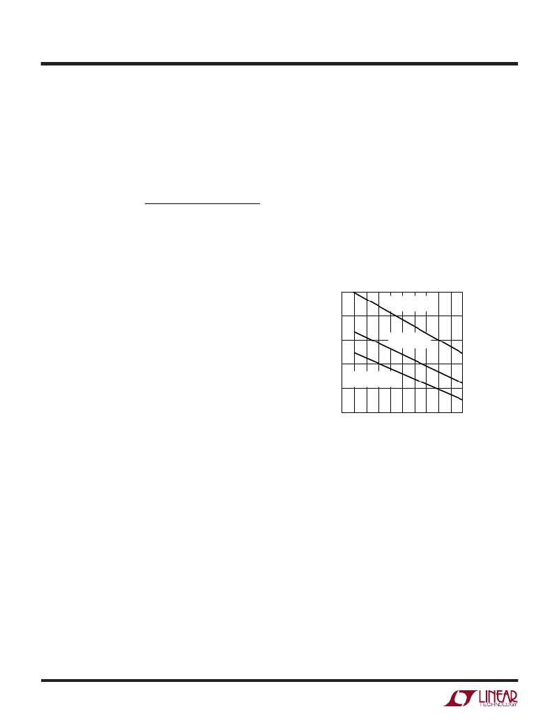
�At� low� supply� voltages,� a� minimum� value� of� C� OUT� is�
�suggested� to� prevent� an� abnormal� low� frequency� operating�
�mode� (see� Figure� 4).� When� C� OUT� is� too� small,� the� output�
�ripple� at� low� frequencies� will� be� large� enough� to� trip� the�
�voltage� comparator.� This� causes� the� Burst� Mode� operation�
�to� be� activated� when� the� LTC1159� would� normally� be� in�
�continuous� operation.� The� effect� is� most� pronounced� with�
�low� values� of� R� SENSE� and� can� be� improved� by� operating� at�
�higher� frequencies� with� lower� values� of� L.� The� output�
�remains� in� regulation� at� all� times.�
�of� life.� This� makes� it� advisable� to� further� derate� the�
�capacitor,� or� to� choose� a� capacitor� rated� at� a� higher�
�temperature� than� required.� Several� capacitors� may� be�
�paralleled� to� meet� size� or� height� requirements� in� the�
�design.� An� additional� 0.1� μ� F� ceramic� capacitor� may� also� be�
�required� on� V� IN� for� high� frequency� decoupling.�
�The� selection� of� C� OUT� is� driven� by� the� required� effective�
�series� resistance� (ESR).� The� ESR� of� C� OUT� must� be� less� than�
�twice� the� value� of� R� SENSE� for� proper� operation� of� the�
�1000�
�800�
�600�
�400�
�200�
�L� =� 50� μ� H�
�R� SENSE� =� 0.02� ?�
�L� =� 25� μ� H�
�R� SENSE� =� 0.02� ?�
�L� =� 50� μ� H�
�R� SENSE� =� 0.05� ?�
�LTC1159:�
�0�
�0�
�1�
�2�
�3�
�4�
�5�
�C� OUT� Required� ESR� <� 2R� SENSE�
�(V� IN� –� V� OUT� )� VOLTAGE� (V)�
�LTC1159� ?� TPC04�
�Optimum� efficiency� is� obtained� by� making� the� ESR� equal� to�
�R� SENSE� .� Manufacturers� such� as� Nichicon,� Chemicon,� and�
�Sprague� should� be� considered� for� high� performance� ca-�
�pacitors.� The� OS-CON� semiconductor� dielectric� capacitor�
�available� from� Sanyo� has� the� lowest� ESR� for� its� size� at� a�
�somewhat� higher� price.� Once� the� ESR� requirement� for�
�C� OUT� has� been� met,� the� RMS� current� rating� generally� far�
�exceeds� the� I� RIPPLE(P-P)� requirement.�
�In� surface� mount� applications,� multiple� capacitors� may�
�have� to� be� paralleled� to� meet� the� capacitance,� ESR� or� RMS�
�current� handling� requirements� of� the� application.� Alumi-�
�num� electrolytic� and� dry� tantalum� capacitors� are� both�
�available� in� surface� mount� configurations.� In� the� case� of�
�tantalum,� it� is� critical� that� the� capacitors� are� surge� tested�
�for� use� in� switching� power� supplies.� An� excellent� choice� is�
�the� AVX� TPS� series� of� surface� mount� tantalums,� available�
�in� case� heights� ranging� from� 2mm� to� 4mm.� For� example,�
�10�
�Figure� 4.� Minimum� Suggested� C� OUT�
�Load� Transient� Response�
�Switching� regulators� take� several� cycles� to� respond� to� a�
�step� in� DC� (resistive)� load� current.� When� a� load� step�
�occurs,� V� OUT� shifts� by� an� amount� equal� to� ?� I� LOAD� ?� ESR,�
�where� ESR� is� the� effective� series� resistance� of� C� OUT� .� ?� I� LOAD�
�also� begins� to� charge� or� discharge� C� OUT� until� the� regulator�
�loop� adapts� to� the� current� change� and� returns� V� OUT� to� its�
�steady-state� value.� During� this� recovery� time� V� OUT� can� be�
�monitored� for� overshoot� or� ringing� which� would� indicate� a�
�stability� problem.� The� I� TH� external� components� shown� in�
�the� Figure� 1� circuit� will� provide� adequate� compensation� for�
�most� applications.�
�A� second,� more� severe� transient� is� caused� by� switching� in�
�loads� with� large� (>1� μ� F)� supply� bypass� capacitors.� The�
�相关PDF资料 |
PDF描述 |
|---|---|
| LTC1159IS-3.3#TR | IC REG CTRLR BUCK PWM CM 16-SOIC |
| RBM31DRSH-S288 | CONN EDGECARD 62POS .156 EXTEND |
| GEC49DRXI-S734 | CONN EDGECARD 98POS DIP .100 SLD |
| RSM18DRSD-S288 | CONN EDGECARD 36POS DIP .156 SLD |
| VE-B7Y-EX-F1 | CONVERTER MOD DC/DC 3.3V 49.5W |
相关代理商/技术参数 |
参数描述 |
|---|---|
| LTC1160CN | 制造商:未知厂家 制造商全称:未知厂家 功能描述:Interface IC |
| LTC1160CS | 制造商:未知厂家 制造商全称:未知厂家 功能描述:Interface IC |
| LTC1160IN | 制造商:未知厂家 制造商全称:未知厂家 功能描述:Interface IC |
| LTC1160IS | 制造商:未知厂家 制造商全称:未知厂家 功能描述:Interface IC |
| LTC1162CN | 制造商:未知厂家 制造商全称:未知厂家 功能描述:Interface IC |
发布紧急采购,3分钟左右您将得到回复。