- 您现在的位置:买卖IC网 > PDF目录15253 > LTC1159IS-5#TR (Linear Technology)IC REG CTRLR BUCK PWM CM 16-SOIC PDF资料下载
参数资料
| 型号: | LTC1159IS-5#TR |
| 厂商: | Linear Technology |
| 文件页数: | 5/20页 |
| 文件大小: | 0K |
| 描述: | IC REG CTRLR BUCK PWM CM 16-SOIC |
| 标准包装: | 2,500 |
| PWM 型: | 电流模式 |
| 输出数: | 1 |
| 频率 - 最大: | 250kHz |
| 占空比: | 100% |
| 电源电压: | 4 V ~ 40 V |
| 降压: | 是 |
| 升压: | 无 |
| 回扫: | 无 |
| 反相: | 无 |
| 倍增器: | 无 |
| 除法器: | 无 |
| Cuk: | 无 |
| 隔离: | 无 |
| 工作温度: | -40°C ~ 85°C |
| 封装/外壳: | 16-SOIC(0.154",3.90mm 宽) |
| 包装: | 带卷 (TR) |
| 其它名称: | LTC1159IS-5TR LTC1159IS5TR |
�� �
�
�LTC1159�
�LTC1159-3.3/LTC1159-5�
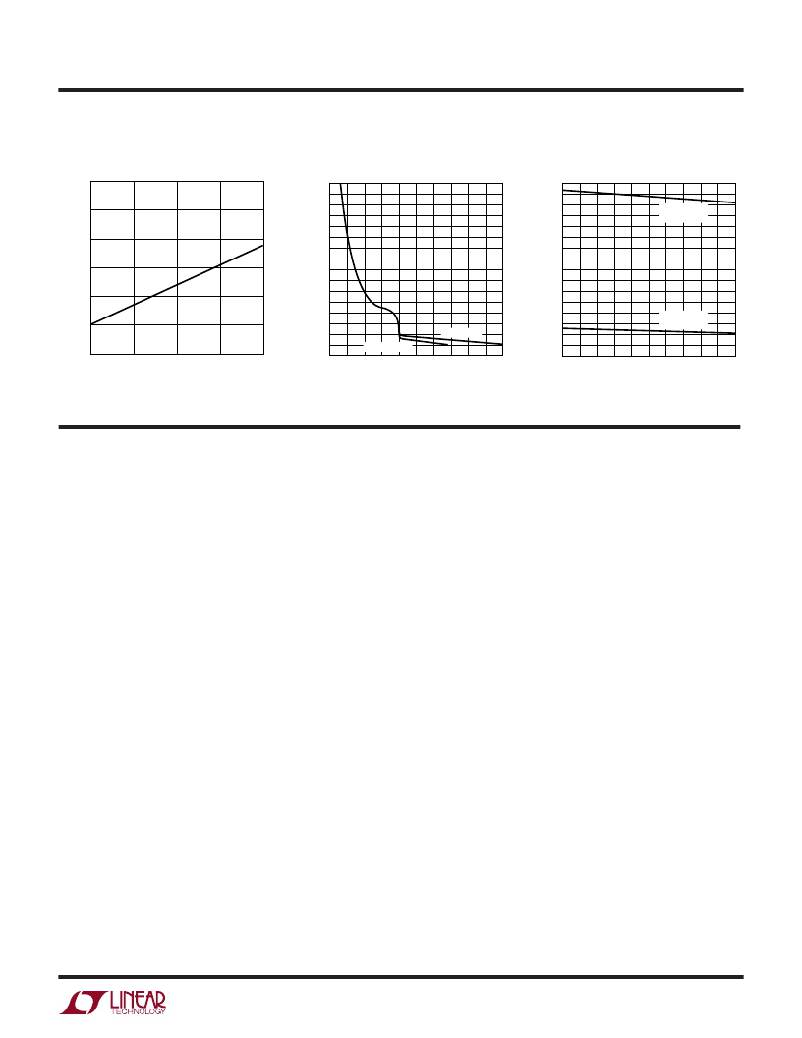
�TYPICAL� PERFOR� A� CE� CHARACTERISTICS�
�600�
�EXTV� CC� Switch� Drop�
�80�
�Off-Time� vs� V� OUT�
�160�
�Current� Sense� Threshold� Voltage�
�500�
�400�
�300�
�200�
�70�
�60�
�50�
�40�
�30�
�20�
�140�
�120�
�100�
�80�
�60�
�40�
�MAXIMUM�
�THRESHOLD�
�MINIMUM�
�100�
�10�
�LTC1159-5�
�20�
�THRESHOLD�
�0�
�0�
�5� 10� 15�
�20�
�0�
�0�
�LTC1159-3.3�
�1� 2�
�3� 4�
�5�
�0�
�0�
�20�
�40�
�60�
�80�
�100�
�SWITCH� CURRENT� (mA)�
�LTC1159� ?� TPC07�
�PI� FU� CTIO� S�
�OUTPUT� VOLTAGE� (V)�
�LTC1159� ?� TPC08�
�TEMPERATURE� (� °� C)�
�LTC1159� ?� TPC09�
�V� IN� :� Main� Supply� Input� Pin.�
�SGND:� Small-Signal� Ground.� Must� be� routed� separately�
�from� other� grounds� to� the� (–)� terminal� of� C� OUT� .�
�PGND:� Driver� Power� Grounds.� Connect� to� source� of� N-�
�channel� MOSFET� and� the� (–)� terminal� of� C� IN� .�
�V� CC� :� Outputs� of� internal� 4.5V� linear� regulator,� EXTV� CC�
�switch,� and� supply� inputs� for� driver� and� control� circuits.�
�The� driver� and� control� circuits� are� powered� from� the� higher�
�of� the� 4.5V� regulator� or� EXTV� CC� voltage.� Must� be� closely�
�decoupled� to� power� ground.�
�C� T� :� External� capacitor� C� T� from� this� pin� to� ground� sets� the�
�operating� frequency.� (The� frequency� is� also� dependent� on�
�the� ratio� V� OUT� /V� IN� .)�
�I� TH� :� Gain� Amplifier� Decoupling� Point.� The� current� com-�
�parator� threshold� increases� with� the� I� TH� pin� voltage.�
�V� FB� :� For� the� LTC1159� adjustable� version,� the� V� FB� pin�
�receives� the� feedback� voltage� from� an� external� resistive�
�divider� used� to� set� the� output� voltage.�
�SENSE� –� :� Connects� to� internal� resistive� divider� which� sets�
�the� output� voltage� in� fixed� output� versions.� The� SENSE� –� pin�
�SENSE� +� :� The� (+)� Input� for� the� Current� Comparator.� A� built-�
�in� offset� between� the� SENSE� +� and� SENSE� –� pins,� in� conjunc-�
�tion� with� R� SENSE� ,� sets� the� current� trip� threshold.�
�N-Gate:� High� Current� Drive� for� the� Bottom� N-Channel�
�MOSFET.� The� N-Gate� pin� swings� from� ground� to� V� CC� .�
�P-Gate:� Level-Shifted� Gate� Drive� Signal� for� the� Top�
�P-Channel� MOSFET.� The� voltage� swing� at� the� P-gate� pin� is�
�from� V� IN� to� V� IN� –� V� CC� .�
�P-Drive:� High� Current� Gate� Drive� for� the� Top� P-Channel�
�MOSFET.� The� P-drive� pin(s)� swing(s)� from� V� CC� to� ground.�
�CAP:� Charge� Compensation� Pin.� A� capacitor� to� V� CC� pro-�
�vides� charge� required� by� the� P-gate� level-shift� capacitor�
�during� supply� transitions.� The� charge� compensation� ca-�
�pacitor� must� be� larger� than� the� gate� drive� capacitor.�
�SHDN1:� This� pin� shuts� down� the� control� circuitry� only� (V� CC�
�is� not� affected).� Taking� SHDN1� pin� high� turns� off� the�
�control� circuitry� and� holds� both� MOSFETs� off.� This� pin�
�must� be� at� ground� potential� for� normal� operation.�
�SHDN2:� Master� Shutdown� Pin.� Taking� SHDN2� high� shuts�
�down� V� CC� and� all� control� circuitry.�
�is� also� the� (–)� input� of� the� current� comparator.�
�5�
�相关PDF资料 |
PDF描述 |
|---|---|
| LTC1159IS-3.3#TR | IC REG CTRLR BUCK PWM CM 16-SOIC |
| RBM31DRSH-S288 | CONN EDGECARD 62POS .156 EXTEND |
| GEC49DRXI-S734 | CONN EDGECARD 98POS DIP .100 SLD |
| RSM18DRSD-S288 | CONN EDGECARD 36POS DIP .156 SLD |
| VE-B7Y-EX-F1 | CONVERTER MOD DC/DC 3.3V 49.5W |
相关代理商/技术参数 |
参数描述 |
|---|---|
| LTC1160CN | 制造商:未知厂家 制造商全称:未知厂家 功能描述:Interface IC |
| LTC1160CS | 制造商:未知厂家 制造商全称:未知厂家 功能描述:Interface IC |
| LTC1160IN | 制造商:未知厂家 制造商全称:未知厂家 功能描述:Interface IC |
| LTC1160IS | 制造商:未知厂家 制造商全称:未知厂家 功能描述:Interface IC |
| LTC1162CN | 制造商:未知厂家 制造商全称:未知厂家 功能描述:Interface IC |
发布紧急采购,3分钟左右您将得到回复。