- 您现在的位置:买卖IC网 > PDF目录9503 > LTC1287CCN8#PBF (Linear Technology)IC DATA ACQ SYS 12BIT 3V 8-DIP PDF资料下载
参数资料
| 型号: | LTC1287CCN8#PBF |
| 厂商: | Linear Technology |
| 文件页数: | 14/16页 |
| 文件大小: | 0K |
| 描述: | IC DATA ACQ SYS 12BIT 3V 8-DIP |
| 标准包装: | 50 |
| 类型: | 数据采集系统(DAS) |
| 分辨率(位): | 12 b |
| 采样率(每秒): | 30k |
| 数据接口: | 串行,并联 |
| 电压电源: | 单电源 |
| 电源电压: | 3V |
| 工作温度: | 0°C ~ 70°C |
| 安装类型: | 通孔 |
| 封装/外壳: | 8-DIP(0.300",7.62mm) |
| 供应商设备封装: | 8-PDIP |
| 包装: | 管件 |
LTC1287
7
1287fa
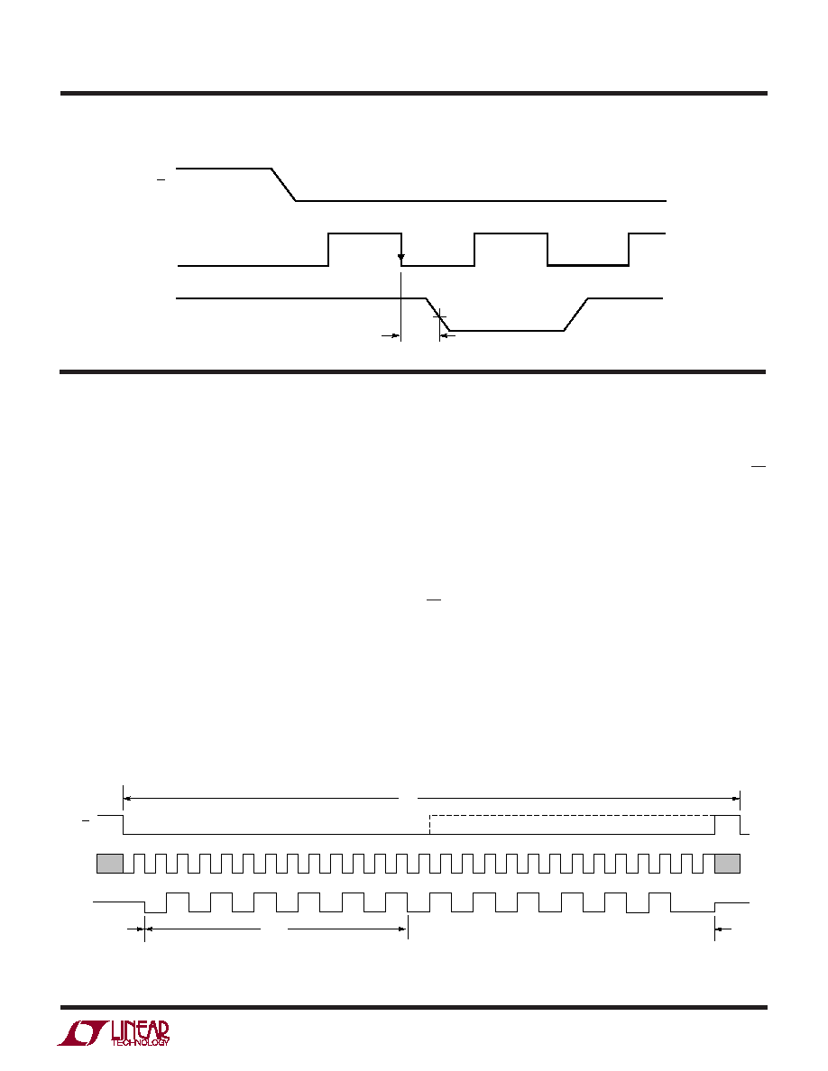
TEST CIRCUITS
Voltage Waveforms for ten
U
S
A
O
PPLICATI
WU
U
I FOR ATIO
The LTC1287 is a data acquisition component which
contains the following functional blocks:
1. 12-bit successive approximation capacitive A/D
converter
2. Analog multiplexer (MUX)
3. Sample-and-hold (S/H)
4. Synchronous, half-duplex serial interface
5. Control and timing logic
DIGITAL CONSIDERATIONS
Serial Interface
The LTC1287 communicates with microprocessors and
other external circuitry via a synchronous, half-duplex,
three-wire serial interface (see Operating Sequence). The
clock (CLK) synchronizes the data transfer with each bit
being transmitted on the falling CLK edge. The LTC1287
does not require a configuration input word and has no DIN
pin. It is permanently configured to have a single differen-
tial input and to operate in unipolar mode. A falling CS
initiates data transfer. The first CLK pulse enables DOUT.
After one null bit, the A/D conversion result is output on the
DOUT line with a MSB-first sequence followed by a LSB-
first sequence. With the half duplex serial interface the
DOUT data is from the current conversion. This provides
easy interface to MSB- or LSB-first serial ports. Bringing
CS high resets the LTC1287 for the next data exchange.
Logic Levels
The logic level standards for this supply range have not
been well defined. What standards that do exist are not
universally accepted. The trip point on the logic inputs of
the LTC1287 is 0.28
× VCC. This makes the logic inputs
compatible with HC-type levels and processors that are
DOUT
0.6V
ten
B11
CS
CLK
LTC1287 TC07
CLK
tCYC
CS
B11
B10
B9
B8
B7
B6
B5
B4
B3
B2
B1
B0
B1
B2
B3
B4
B5
B6
B7
B8
B9
B10
B11
tCONV
DOUT
Hi-Z
tSMPL
LTC1287 F01
Figure 1. LTC1287 Operating Sequence
相关PDF资料 |
PDF描述 |
|---|---|
| LTC1287CCN8 | IC DATA ACQ SYS 12BIT 3V 8-DIP |
| VI-25L-MY-S | CONVERTER MOD DC/DC 28V 50W |
| VI-253-MY-S | CONVERTER MOD DC/DC 24V 50W |
| AD2S1210BSTZ | IC CONV R/D 10-16BIT 48-LQFP |
| V110A24M300B | CONVERTER MOD DC/DC 24V 300W |
相关代理商/技术参数 |
参数描述 |
|---|---|
| LTC1288CN8 | 功能描述:IC A/D CONV SAMPLING 12BIT 8-DIP RoHS:否 类别:集成电路 (IC) >> 数据采集 - 模数转换器 系列:- 标准包装:1,000 系列:- 位数:16 采样率(每秒):45k 数据接口:串行 转换器数目:2 功率耗散(最大):315mW 电压电源:模拟和数字 工作温度:0°C ~ 70°C 安装类型:表面贴装 封装/外壳:28-SOIC(0.295",7.50mm 宽) 供应商设备封装:28-SOIC W 包装:带卷 (TR) 输入数目和类型:2 个单端,单极 |
| LTC1288CN8#PBF | 功能描述:IC A/D CONV SAMPLING 12BIT 8-DIP RoHS:是 类别:集成电路 (IC) >> 数据采集 - 模数转换器 系列:- 其它有关文件:TSA1204 View All Specifications 标准包装:1 系列:- 位数:12 采样率(每秒):20M 数据接口:并联 转换器数目:2 功率耗散(最大):155mW 电压电源:模拟和数字 工作温度:-40°C ~ 85°C 安装类型:表面贴装 封装/外壳:48-TQFP 供应商设备封装:48-TQFP(7x7) 包装:Digi-Reel® 输入数目和类型:4 个单端,单极;2 个差分,单极 产品目录页面:1156 (CN2011-ZH PDF) 其它名称:497-5435-6 |
| LTC1288CN8PBF | 制造商:Linear Technology 功能描述:LTC1288CN8PBF |
| LTC1288CS8 | 功能描述:IC A/D CONV SAMPLING 12BIT 8SOIC RoHS:否 类别:集成电路 (IC) >> 数据采集 - 模数转换器 系列:- 标准包装:1,000 系列:- 位数:16 采样率(每秒):45k 数据接口:串行 转换器数目:2 功率耗散(最大):315mW 电压电源:模拟和数字 工作温度:0°C ~ 70°C 安装类型:表面贴装 封装/外壳:28-SOIC(0.295",7.50mm 宽) 供应商设备封装:28-SOIC W 包装:带卷 (TR) 输入数目和类型:2 个单端,单极 |
| LTC1288CS8#PBF | 功能描述:IC A/D CONV SAMPLING 12BIT 8SOIC RoHS:是 类别:集成电路 (IC) >> 数据采集 - 模数转换器 系列:- 标准包装:1,000 系列:- 位数:16 采样率(每秒):45k 数据接口:串行 转换器数目:2 功率耗散(最大):315mW 电压电源:模拟和数字 工作温度:0°C ~ 70°C 安装类型:表面贴装 封装/外壳:28-SOIC(0.295",7.50mm 宽) 供应商设备封装:28-SOIC W 包装:带卷 (TR) 输入数目和类型:2 个单端,单极 |
发布紧急采购,3分钟左右您将得到回复。