- 您现在的位置:买卖IC网 > PDF目录9503 > LTC1287CCN8#PBF (Linear Technology)IC DATA ACQ SYS 12BIT 3V 8-DIP PDF资料下载
参数资料
| 型号: | LTC1287CCN8#PBF |
| 厂商: | Linear Technology |
| 文件页数: | 6/16页 |
| 文件大小: | 0K |
| 描述: | IC DATA ACQ SYS 12BIT 3V 8-DIP |
| 标准包装: | 50 |
| 类型: | 数据采集系统(DAS) |
| 分辨率(位): | 12 b |
| 采样率(每秒): | 30k |
| 数据接口: | 串行,并联 |
| 电压电源: | 单电源 |
| 电源电压: | 3V |
| 工作温度: | 0°C ~ 70°C |
| 安装类型: | 通孔 |
| 封装/外壳: | 8-DIP(0.300",7.62mm) |
| 供应商设备封装: | 8-PDIP |
| 包装: | 管件 |
14
LTC1287
1287fa
U
S
A
O
PPLICATI
WU
U
I FOR ATIO
curve of Noise Error vs Reference Voltage shows the
LSB contribution of this 200
V of noise.
For operation with a 2.5V reference, the 200
V noise is
only 0.32LSB peak-to-peak. Here the LTC1287 noise
will contribute virtually no uncertainty to the output
code. For reduced references, the noise may become a
significant fraction of an LSB and cause undesirable
jitter in the output code. For example, with a 1.25V
reference, this 200
V noise is 0.64LSB peak-to-peak.
This will reduce the range of input voltages over which
a stable output code can be achieved by 0.64LSB. Now
averaging readings may be necessary.
This noise data was taken in a very clean test fixture.
Any setup induced noise (noise or ripple on VCC, VREF
or VIN) will add to the internal noise. The lower the
reference voltage used, the more critical it becomes to
have a noise-free setup.
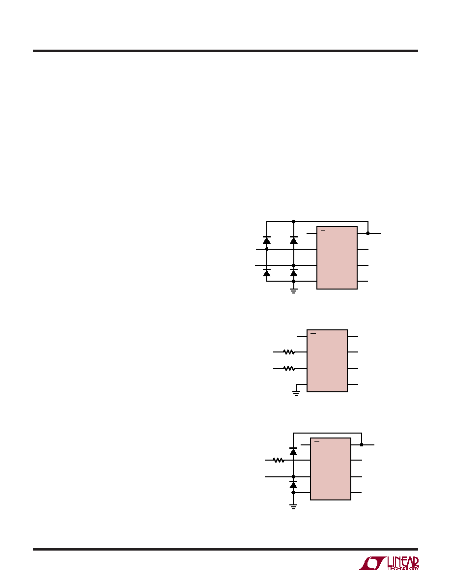
Overvoltage Protection
Applying signals to the LTC1287’s analog inputs that
exceed the positive supply or that go below ground will
degrade the accuracy of the A/D and possibly damage
the device. For example this condition would occur if a
signal is applied to the analog inputs before power is
applied to the LTC1287. Another example is the input
source operating from different supplies of larger value
than the LTC1287. These conditions should be pre-
vented either with proper supply sequencing or by use
of external circuitry to clamp or current limit the input
source. There are two ways to protect the inputs. In
Figure 15 diode clamps from the inputs to VCC and GND
are used. The second method is to put resistors in
series with the analog inputs for current limiting. Limit
the current to 15mA per channel. The +IN input can
accept a resistor value of 1k but the –IN input cannot
accept more than 200
when clocked at its maximum
clock frequency of 500kHz. If the LTC1287 is clocked at
the maximum clock frequency and 200
is not enough
to current limit the input source then the clamp diodes
are recommended (Figures 16 and 17). The reason for
the limit on the resistor value is the MSB bit test is
affected by the value of the resistor placed at the –IN
input (see discussion on Analog Inputs and the Typical
Performance Characteristics curve of Maximum CLK
Frequency vs Source Resistance).
If VCC and VREF are not tied together, then VCC should
be turned on first, then VREF. If this sequence cannot be
met, connecting a diode from VREF to VCC is recom-
mended (see Figure 18).
Because a unique input protection structure is used on
the digital input pins, the signal levels on these pins can
exceed the device VCC without damaging the device.
Figure 17. Overvoltage Protection for Inputs
+3V
LTC1287 F17
+IN
GND
VREF
DOUT
CLK
VCC
CS
–IN
LTC1287
1N4148 DIODES
1k
Figure 16. Overvoltage Protection for Inputs
+3V
LTC1287 F16
+IN
GND
VREF
DOUT
CLK
VCC
CS
–IN
200
1k
LTC1287
Figure 15. Overvoltage Protection for Inputs
+3V
LTC1287 F15
+IN
GND
VREF
DOUT
CLK
VCC
CS
–IN
1N4148 DIODES
LTC1287
相关PDF资料 |
PDF描述 |
|---|---|
| LTC1287CCN8 | IC DATA ACQ SYS 12BIT 3V 8-DIP |
| VI-25L-MY-S | CONVERTER MOD DC/DC 28V 50W |
| VI-253-MY-S | CONVERTER MOD DC/DC 24V 50W |
| AD2S1210BSTZ | IC CONV R/D 10-16BIT 48-LQFP |
| V110A24M300B | CONVERTER MOD DC/DC 24V 300W |
相关代理商/技术参数 |
参数描述 |
|---|---|
| LTC1288CN8 | 功能描述:IC A/D CONV SAMPLING 12BIT 8-DIP RoHS:否 类别:集成电路 (IC) >> 数据采集 - 模数转换器 系列:- 标准包装:1,000 系列:- 位数:16 采样率(每秒):45k 数据接口:串行 转换器数目:2 功率耗散(最大):315mW 电压电源:模拟和数字 工作温度:0°C ~ 70°C 安装类型:表面贴装 封装/外壳:28-SOIC(0.295",7.50mm 宽) 供应商设备封装:28-SOIC W 包装:带卷 (TR) 输入数目和类型:2 个单端,单极 |
| LTC1288CN8#PBF | 功能描述:IC A/D CONV SAMPLING 12BIT 8-DIP RoHS:是 类别:集成电路 (IC) >> 数据采集 - 模数转换器 系列:- 其它有关文件:TSA1204 View All Specifications 标准包装:1 系列:- 位数:12 采样率(每秒):20M 数据接口:并联 转换器数目:2 功率耗散(最大):155mW 电压电源:模拟和数字 工作温度:-40°C ~ 85°C 安装类型:表面贴装 封装/外壳:48-TQFP 供应商设备封装:48-TQFP(7x7) 包装:Digi-Reel® 输入数目和类型:4 个单端,单极;2 个差分,单极 产品目录页面:1156 (CN2011-ZH PDF) 其它名称:497-5435-6 |
| LTC1288CN8PBF | 制造商:Linear Technology 功能描述:LTC1288CN8PBF |
| LTC1288CS8 | 功能描述:IC A/D CONV SAMPLING 12BIT 8SOIC RoHS:否 类别:集成电路 (IC) >> 数据采集 - 模数转换器 系列:- 标准包装:1,000 系列:- 位数:16 采样率(每秒):45k 数据接口:串行 转换器数目:2 功率耗散(最大):315mW 电压电源:模拟和数字 工作温度:0°C ~ 70°C 安装类型:表面贴装 封装/外壳:28-SOIC(0.295",7.50mm 宽) 供应商设备封装:28-SOIC W 包装:带卷 (TR) 输入数目和类型:2 个单端,单极 |
| LTC1288CS8#PBF | 功能描述:IC A/D CONV SAMPLING 12BIT 8SOIC RoHS:是 类别:集成电路 (IC) >> 数据采集 - 模数转换器 系列:- 标准包装:1,000 系列:- 位数:16 采样率(每秒):45k 数据接口:串行 转换器数目:2 功率耗散(最大):315mW 电压电源:模拟和数字 工作温度:0°C ~ 70°C 安装类型:表面贴装 封装/外壳:28-SOIC(0.295",7.50mm 宽) 供应商设备封装:28-SOIC W 包装:带卷 (TR) 输入数目和类型:2 个单端,单极 |
发布紧急采购,3分钟左右您将得到回复。