参数资料
| 型号: | LTC1297BCN8 |
| 厂商: | Linear Technology |
| 文件页数: | 11/24页 |
| 文件大小: | 0K |
| 描述: | IC DATA ACQ SYSTEM 12BIT 8-DIP |
| 标准包装: | 50 |
| 类型: | 数据采集系统(DAS) |
| 分辨率(位): | 12 b |
| 采样率(每秒): | 60k |
| 数据接口: | 串行,并联 |
| 电压电源: | 单电源 |
| 电源电压: | 5V |
| 工作温度: | 0°C ~ 70°C |
| 安装类型: | 通孔 |
| 封装/外壳: | 8-DIP(0.300",7.62mm) |
| 供应商设备封装: | 8-PDIP |
| 包装: | 管件 |
19
LTC1292/LTC1297
12927fb
is reduced. The typical performance characteristics
curve of Noise Error vs Reference Voltage shows the
LSB contribution of this 200
V of noise.
For operation with a 5V reference, the 200
V noise is
only 0.16LSB peak-to-peak. Here the LTC1292/LTC1297
noise will contribute virtually no uncertainty to the
output code. For reduced references, the noise may
become a significant fraction of an LSB and cause
undesirable jitter in the output code. For example, with
a 1.25V reference, this 200
V noise is 0.64LSB peak-
to-peak. This will reduce the range of input voltages
over which a stable output code can be achieved by
0.64LSB. Now, averaging readings may be necessary.
This noise data was taken in a very clean test fixture.
Any setup induced noise (noise or ripple on VCC, VREF
or VIN) will add to the internal noise. The lower the
reference voltage used, the more critical it becomes to
have a noise-free setup.
Gain Error Due to Reduced VREF
The gain error of the LTC1292/LTC1297 is very good
over a wide range of reference voltages. The error
component that is seen in the typical performance
characteristics curve Change in Gain Error vs Refer-
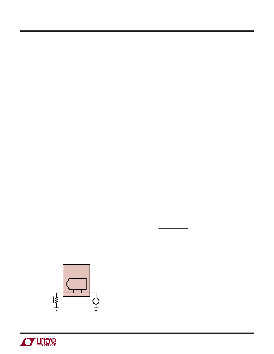
ence Voltage is due to the voltage drop on the GND pin
from the device to the ground plane. To minimize this
error the LTC1292/LTC1297 should be soldered di-
rectly onto the PC board. The internal reference point
for VREF is tied to GND. Any voltage drop in the GND pin
will make the reference voltage, internal to the device,
less than what is applied externally (Figure 19). This
drop is typically 420
V due to the product of the pin
resistance (RPIN) and the LTC1292/LTC1297 supply
U
S
A
O
PPLICATI
WU
U
I FOR ATIO
This is the effective number of bits (ENOB). For the
example shown in Figures 20a and 20b, N = 11.8 bits
and 9.9 bits, respectively. Figure 21 shows a plot of
ENOB as a function of input frequency. The 2nd har-
monic distortion term accounts for the degradation of
the ENOB as fIN approaches fS/2.
Figure 22 shows an FFT plot of the output spectrum for
two tones applied to the input of the A/D. Nonlinearities
in the A/D will cause distortion products at the sum and
difference frequencies of the fundamentals and prod-
ucts of the fundamentals. This is classically referred to
as intermodulation distortion (IMD).
LTC1292
LTC1297
REF+
RPIN
ICC
DAC
REF–
VREF
GND
LTC1292/7 F19
± REFERENCE
VOLTAGE
current. For example, with VREF = 1.25V this will result
in a gain error change of –1.0LSB from the gain error
measured with VREF = 5V.
LTC1292 AC Characteristics
Two commonly used figures of merit for specifying the
dynamic performance of the A/Ds in digital signal
processing applications are the Signal-to-Noise Ratio
(SNR) and the “Effective Number of Bits (ENOB).” SNR
is the ratio of the RMS magnitude of the fundamental to
the RMS magnitude of all the non-fundamental signals
up to the Nyquist frequency (half the sampling fre-
quency). The theoretical maximum SNR for a sine wave
input is given by:
SNR = (6.02N + 1.76dB)
where N is the number of bits. Thus the SNR depends
on the resolution of the A/D. For an ideal 12-bit A/D the
SNR is equal to 74dB. Fast Fourier Transform (FFT)
plots of the output spectrum of the LTC1292 are shown
in Figures 20a and 20b. The input (fIN) frequencies are
1kHz and 28kHz with the sampling frequency (fS) at
58.8 kHz. The SNRs obtained from the plots are 73.0dB
and 61.5dB.
By rewriting the SNR expression it is possible to obtain
the equivalent resolution based on the SNR measure-
ment.
N
SNR
dB
=
–.
.
176
602
Figure 19. Parasitic Resistance in GND Pin
相关PDF资料 |
PDF描述 |
|---|---|
| VI-B1K-IU-F2 | CONVERTER MOD DC/DC 40V 200W |
| LTC6905CS5-96#TRPBF | IC OSC SILICON 96MHZ TSOT23-5 |
| VI-B1K-IU-F1 | CONVERTER MOD DC/DC 40V 200W |
| AD7890BRZ-10 | IC DAS 12BIT 8CH 24-SOIC |
| LTC6905CS5-133#TRMPBF | IC OSC SILICON 133MHZ TSOT23-5 |
相关代理商/技术参数 |
参数描述 |
|---|---|
| LTC1297BCN8#PBF | 功能描述:IC DATA ACQ SYSTEM 12BIT 8-DIP RoHS:是 类别:集成电路 (IC) >> 数据采集 - ADCs/DAC - 专用型 系列:- 产品培训模块:Lead (SnPb) Finish for COTS Obsolescence Mitigation Program 标准包装:50 系列:- 类型:数据采集系统(DAS) 分辨率(位):16 b 采样率(每秒):21.94k 数据接口:MICROWIRE?,QSPI?,串行,SPI? 电压电源:模拟和数字 电源电压:1.8 V ~ 3.6 V 工作温度:-40°C ~ 85°C 安装类型:表面贴装 封装/外壳:40-WFQFN 裸露焊盘 供应商设备封装:40-TQFN-EP(6x6) 包装:托盘 |
| LTC1297CCJ8 | 制造商:Linear Technology 功能描述:ADC Single SAR 50ksps 12-bit Serial 8-Pin CDIP |
| LTC1297CCN8 | 功能描述:IC DATA ACQ SYSTEM 12BIT 8-DIP RoHS:否 类别:集成电路 (IC) >> 数据采集 - ADCs/DAC - 专用型 系列:- 产品培训模块:Lead (SnPb) Finish for COTS Obsolescence Mitigation Program 标准包装:50 系列:- 类型:数据采集系统(DAS) 分辨率(位):16 b 采样率(每秒):21.94k 数据接口:MICROWIRE?,QSPI?,串行,SPI? 电压电源:模拟和数字 电源电压:1.8 V ~ 3.6 V 工作温度:-40°C ~ 85°C 安装类型:表面贴装 封装/外壳:40-WFQFN 裸露焊盘 供应商设备封装:40-TQFN-EP(6x6) 包装:托盘 |
| LTC1297CCN8#PBF | 功能描述:IC DATA ACQ SYSTEM 12BIT 8-DIP RoHS:是 类别:集成电路 (IC) >> 数据采集 - ADCs/DAC - 专用型 系列:- 产品培训模块:Lead (SnPb) Finish for COTS Obsolescence Mitigation Program 标准包装:50 系列:- 类型:数据采集系统(DAS) 分辨率(位):16 b 采样率(每秒):21.94k 数据接口:MICROWIRE?,QSPI?,串行,SPI? 电压电源:模拟和数字 电源电压:1.8 V ~ 3.6 V 工作温度:-40°C ~ 85°C 安装类型:表面贴装 封装/外壳:40-WFQFN 裸露焊盘 供应商设备封装:40-TQFN-EP(6x6) 包装:托盘 |
| LTC1297CCN8PBF | 制造商:Linear Technology 功能描述:LTC1297CCN8PBF |
发布紧急采购,3分钟左右您将得到回复。